Epitaxial Films of Faas and Fan on Fianit Substrates
- PDF / 1,032,127 Bytes
- 6 Pages / 414.72 x 648 pts Page_size
- 38 Downloads / 363 Views
A.N.BUZYNIN*, V.V.OSIKO*, E.E. LOMONOVA*, YU.N.BUZYNIN**, AND A.S.USIKOV*** *General Physics Institute of Russian Academy of Sciences, 38 Vavilov st., Moscow Russia, [email protected]. **Institute117942, for Physics of Microstructures of RAS, 46 Ulianov st., Nyzhny Novgorod, 603600, Russia ***Physico-Technical Institute of RAS, 26 Polytechnicheskaya st, 194021, Russia ABSTRACT Subrmicron heteroepitaxial GaAs and GaN films were grown by both conventional MOCVD and > technique [5]. It is based on covering of the YSZ wafer with the thin film of A component, with subsequent saturating the film by corresponding B component up to the formation of a ArBV continuous layer. After that the AraBV films were grown to the needed
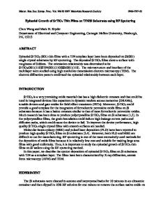
thickness. Fig. 1 shows SEM micrographs of GaAs films prepared by both conventional MOCVD and capillary epitaxy technique at the initial stage of growth and NFhJ graphoepitaxy on amorphous Al substrate. The formation of layers in both capillary epitaxy and graphoepitaxy teclhique take place from created and coalescence of three dimensional nuclea.,As in the case of graphoepitaxy [8] the use of capillary forces at the first heteroepitaxial stage of the GaAs/YSZ film formation resulted in following sequels: (1)-epitaxial nuclea density increased; (2)-the nucleus dimension decreased; (3)-the nucleus habit became more flat; (4)-the epitexial orientation of the nuclea improved. As a result the minimum GaAs/YSZ film thickness was decreased to 50 nm, structure perfection and surface morphology of the films were improved. The single crystalline GaAs on YSZ 50-500 nm thick films were prepared. The submicron GaAs films grown by capillary epitaxy technique had high resistance. For n-type GaAs films Sill4 was used as dopant source. Electron concentration into the films was in the range of 5.1016 to 5.10"7 cm-3. SIMS date showed that background of impurities concentration was similar to that in
419
GaAs/GaAs films. The layer -by-layer SiMS analysis indicated the uniform distribution of impurities in the GaAs films and sharp distribution of Zr, 0 and Y across the film-substrate interface. GaAs 600sek
a
b GaAs 60sek
NH4J
c
d
Fig. I.SEM micrographs of GaAs films prepared by both using convention MOCVD (a) and capillary epitaxy MOCVD(b) technique at the initial stage of epitaxy (60s after procedure beginning, 20000x) and NH 4J graphoepitaxy on amorphous Al substrate without ( c ) and using(d) surface active substance (100x). According to fig. 1 the better wetting of substrate the better films structure both for graphoepitaxy of NH14 on Al and capillary and capillary epitaxy GaAs on YSZ.
GaN Films on YSZ GaN films on YSZ substrates were grown both conventional MOVPE [9] and ocapillary epitaxy)> [5] technique similarly to GaAs films. The thin (-50nm) Ga
420
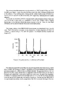
layer on YSZ substrate was predeposited by MOD technique before the GaN MOVPE growth in TMG-NH 3-H2 system at 1025 0C in the case of «(capillary epitaxyi> technique using. The GaN films had a mosaic structure. Typical examples of PL spectra of undoped Ga
Data Loading...