Epitaxial Growth and Properties of Mg-Doped Gan Film Produced by Atmospheric MOCVD System With Three Layered Lammar Flow
- PDF / 369,447 Bytes
- 6 Pages / 414.72 x 648 pts Page_size
- 114 Downloads / 293 Views
Mat. Res. Soc. Symp. Proc. Vol. 482 ©1998 Materials Research Society
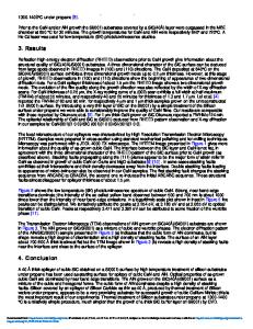
GaN films. EXPERIMENTAL The Mg-doped GaN films were grown by atmospheric horizontal MOCVD system with three layered laminar flow gas injection [81 on sapphire (0001) substrates with 20nm GaN buffer layers. In this MOCVD system, NH 3, organometals and topflow gas were separately injected into the flow liner and mixed near the substrate. By this mixing method, parasitic reaction between NH 3 and organometals are suppressed. Trimethylgallium (TMG) and high purity ammonia (H20:67ppb) were used as precursors. Moisture in the NH 3 was measured by laser absorption spectroscopy (LAMBDASCAN; Nippon Sanso Co.)[9]. Bis-cyclopentadienyl magnesium (Cp2Mg) was used as Mg source. The growth conditions are shown in Table 1.The thickness of the epitaxial Mg-doped layer was 2.7pm. Following the growth of the epitaxial Mgdoped GaN layer, post growth thermal annealing was done in N 2 ambient for 20min at 8000 C. Hall measurement samples were then prepared by depositing Ni contact to 1cm 2 section of each wafer. Carrier densities and mobilities were meaured by van der Pauw method. The most likely impurities, such as H, 0, C and Si were measured by SIMS. The detection limit of those elements were 2 X 10¹⁸/cm3, 2 X 10¹⁷/cm 3, 1 X 10¹⁷/cm 3 and 2 X 10¹⁶/cm 3, respectively. Table 1 Mg-doped GaN and GaN buffer growth conditions temp.
GaN buffer Mg-doped GaN
0 (C 450 1000-1025
TMG
NIL
Cpz1Mg
(pmol/mm) (pmol/min) 44 0.05-9 88
(SLM) 5 8
I%
subflow
time
(SWM) 15 12
(SLM) 15 14
(min) 1.1 60.0
RESULTS AND DISCUSSION Figure 1 shows SIMS depth profile of an unintentionally doped as grown GaN film. The surface morphology of the unintentionally doped GaN film is mirrorlike and the double crystal x-ray diffraction rocking curve (DCXRD) FWHM for (0002) diffraction is 240arcsec. Typical electrical properties of unintentionally doped GaN film is n-type with a electron mobility of 500cm 2N s at a carrier concentration of 6X 10¹⁶/cm 3 .The concentration of H, C, 0 and Si is 3X 10¹⁸/cm 3, 6X016/cm 3 ,2X1017/cm 3and 2Xl016/cm 3, respectively. If assume an oxygen donor level of 78meV and no compensation, the resulting Fermi energy would lie at 39meV below the conduction band edge, that bring about a free electron concentration of nearly 5X 10¹⁶/cm3 for 2 X10¹⁷/cm 3 oxygen. Therefore, the residual oxygen and Si can play an important role in our undoped GaN. Figure 2 shows the Mg concentration and carrier concentration as a function of Cp2,Mg flow rate on Mg-doped GaN after post growth annealing. In the figure, Mg-doped GaN films were grown at 1000°C. It is found that the Mg concentration is proportional to the Cp2Mg flow rate from 0.05 to 0.5Omol/min and saturates at about 2X 10²⁰/cm 3 with higher Cp2Mg flow rate more than about 0.5 jimol/min. Conduction type changes from p-type to n-type around the Cp2]Mg flow rate of 0.5pmol. Hole carrier concentration of the film grown at the Cp2Mg flow rate of O.lpmol/min is 8X10¹⁷/cm 3.
114
1021
-
1021
020 19
n
0~109
a) -
r
en
n
Data Loading...