Epitaxial Growth of III-Nitride Layers on Aluminum Nitride Substrates
- PDF / 1,211,653 Bytes
- 6 Pages / 417.6 x 639 pts Page_size
- 76 Downloads / 412 Views
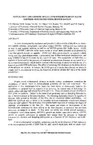
CHARACTERIZATION AND ANALYSIS In Fig. 1, an AFM image of an AIN substrate is shown prior to epitaxial growth. This particular substrate was cut so as to expose the (1120) plane of atoms (the a-face) and was misoriented by less than 1'. It can be seen that substrate surface is nearly atomically flat. Examination of the substrate over a wider area indicates that all evidence of mechanical damage (scratches, etc.) has been removed unlike prior work [3] where micro scratches were observed on the substrate surface after just a mechanical polish. We do observe pit-like defects which may be associated with dislocations intersecting the surface but their origin has not been convincingly determined at this time. Their density is approximately 3x 103 cm-2.
Fig. 1: An AFM image of the bare AIN substrate prior to growth.
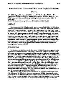
In Fig. 2, an AFM image of a 0.7-1am-thick AIN epitaxial layer, grown on a slightly vicinal AIN substrate, is shown. Atomic steps seem to have organized into semi-regular arrays during
growth giving rise to a grating effect across the surface. The height of the step bunches is approximately 4 nm. The density of defects across the surface, observed with AFM, increased by approximately 1 order of magnitude from the clean substrate. This increase includes the appearance of short line-like defects that were not observed on the original substrate. The origin of these defects is still being investigated.
Fig. 2: An AFM image of a 0.7-Jim-thick epitaxial AIN layer grown on the a-face of an AIN substrate. We have also performed AFM characterization of the surface of a I -Jim-thick epitaxial film of A1. 5Ga.5 N. This film showed a much rougher surface morphology even though the epitaxial quality as determined by x-ray diffraction and ion channeling was very good as discussed below. The surface was found to have many mounds on the surface with approximately 30' facet angles.
Of course, it should also be noted that the growth process has not yet been optimized for growth of AIGa1 _,N alloy layers. Rutherford backscattering/ion channeling measurements were used to determine the crystal quality of the original substrate, the epitaxial AIN layer and the epitaxial AI.5 Ga.5N layer. The results from the later two layers are shown in Figs. 3 and 4. These measurements were performed at the SUNY-Albany Dynamatron accelerator with 2 MeV He 4 ions. The minimum yield was measured along the [1010] axis, which is perpendicular to the (1120) surface plane of this substrate. We obtained a channeling minimum yield Xmin of 1.5% for both the AIN substrate and for the AIN epitaxial layer. The Xmin is the ratio of the backscattering yield along the crystallographic axis compared to the scattering yield along a random direction and a value of 1.5% indicates excellent crystal quality (see, for example, ref. 4 where a y of 2.1% was measured on a high quality, 3-1 tm-thick GaN layer grown under optimal conditions on sapphire). The Xmin measured for the 1-im-thick AI*5Ga 5N layer was 2.2%, which is still excellent even though the growth p
Data Loading...