Equilibration in Amorphous Silicon Nitride Alloys
- PDF / 396,774 Bytes
- 6 Pages / 414.72 x 648 pts Page_size
- 42 Downloads / 435 Views
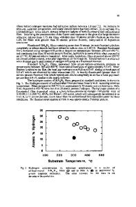
SAMPLE PREPARATION All the samples were deposited from mixtures of ammonia and silane, with a total flow rate of 40 sccm, in a chamber pumped to 150 mTorr. The reactor was a standard parallel plate, radial flow design with a heated stage; the rf supplies were operated at 13.56 MHz, at a power density of 3.5 mW/cm 3 and the deposition temperature was varied from 150 TC up to 600 TC. The ratio of ammonia to silane was varied from 0 up to 2.0. Sample composition was determined by XPS' 5 and it was found that over most of the temperature range, [N]/[Si] = 0.3[NH 3]/[SiH4]. Samples deposited below 180 TC tended to be depleted in nitrogen. Thickness was monitored by Dektak profilometry on samples into which a grating pattern had been etched. PDS samples were deposited to a thickness of 2.5 - 3.5 g.tm on quartz substrates, while FT-IR samples were 0.3 - 0.5 jtm films on polished c-Si substrates. PDS RESULTS The PDS technique16 has become popular in recent years as a method for probing the subgap state distribution in amorphous semiconductors. Although some doubt has been raised over the validity of the underlying theory with respect to the detemination of defect densities '7, in general the empirical agreement between PDS derived results and those obtained from other measurements is satisfactory 9 . The PDS system used was a computer controlled version of the standard design' 6. Measurements were made over the range 300 - 1100 nm, using a single diffraction grating. The sample was positioned inside a quartz cuvette filled with CC14 and mounted on an X-Y-O vernier table to allow fine positioning with respect to the probe laser beam. The films were sufficiently thick (>2.5 pm) that no fringing was observed on the Urbach edge and therefore unambiguous extraction of the Urbach parameter E. was straightforward. The deposition temperature dependence of the Urbach slopes for four series of Urbach Slope (meV) nitride films is shown in figure 1. For each 160 series, three distinct regions of behaviour are 0.08 evident. At low growth temperatures Eo falls o08 140 ý At intermediate growth quite rapidly. 0.15 temperatures, Eo varies much more slowly, 120 1 0.3 although for each series a reproducible -"-100 shallow minimum value is observed. At 0.6 high growth temperatures E0 increases quite %K * 80 rapidly. Similar three-part behaviour has been reported for a-Si' 8, but is not shown in 60 the data shown by Stutzmann 9. 40 The minimum for undoped silicon is 500 200 300 400 widely published to lie in the range 230 Deposition Temp. (*C) 250TC. For the nitrides in the present work this rises to 300 TC for x = 0.08, -365 TC for Figure 1 Deposition temperature dependence of the Urbach slope parameter. x = 0.15 and to 420 TC for x = 0.3, before The dashed line is from Stutzmann's fit to appearing to fall again to -300 TC for x = 0.6 various a-Si samples8 . (where x = [N]/[Si]).
350
3
The defect density was determined by integrating the sub-bandgap excess absorption coefficient' 6. Figure 2 illustrates the deposition temperature depende
Data Loading...