Evidence of the De-Multiplication Interactions Between Threading Dislocations in GaN Films Grown on (0001) Sapphire Subs
- PDF / 414,754 Bytes
- 6 Pages / 612 x 792 pts (letter) Page_size
- 32 Downloads / 317 Views
0994-F03-09
Evidence of the De-Multiplication Interactions Between Threading Dislocations in GaN Films Grown on (0001) Sapphire Substrates Cheng-Liang Wang, and Jyh-Rong Gong Department of Physics, National Chung Hsing University, Taichung City, 402, Taiwan ABSTRACT We report the observation of threading dislocation de-multiplication process by transmission electron microscopy (TEM). The GaN films used in this study were grown on (0001) sapphire substrates with LT-GaN buffer layers by reduced pressure organometallic vapor phase epitaxy. By using g
.b = 0 invisibility criterion, it was found that some of TDs were de-multiplicated by
interactions among themselves. In particular, type a+c TDs were found to nucleate through the interactions between type a and type c TDs in GaN near the GaN/sapphire interface so that the de-multiplication of TDs in GaN films was achieved.
INTRODUCTION It is well known that dislocations serve as non-radiative recombination centers for minority carriers in semiconductors. Despite the influence of threading dislocations (TDs) in GaN-based light emitting diodes (LEDs) is not prominent, the demand of high power LED chips for solid state lightings may need further reduction of TD density in GaN-based structures. Many activities have been conducted to reduce TD density in a GaN film. In wurtzite GaN films, three types of perfect dislocations have been identified as type a, type c and type a+c with the Burgers vectors being 1/ 3 < 1120 > , < 0001 > and 1/ 3 < 1123 > , respectively [1]. It has been reported that the reduction
of TD density in a GaN film can be achieved by annihilation and de-multiplication processes [2]. Although there are reports revealing the TD reduction processes [3], few efforts have addressed how TDs in GaN films are de-multiplicated. In this report, we employed transmission electron
microscopy (TEM) to unambiguously identify the de-multiplication interactions of TDs in GaN films grown on the (0001) sapphire substrates.
EXPERIMENT The GaN films used in this study were grown on (0001) sapphire substrates with LT-GaN buffer layers by reduced pressure organometallic vapor phase epitaxy. In this case, 4 µm-thick GaN films were directly deposited on the (0001) sapphire substrates. A JEOL 1200 EXII TEM was employed for the identification of the Burgers vectors of TDs in the GaN films. The TEM specimens were prepared by using a Gatan 600-DIF argon ion milling equipment.
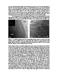
RESULTS AND DISCUSSION Figure 1 shows a cross-sectional TEM (XTEM) micrograph of a GaN film. In this case, one
Figure 1. Typical XTEM images of a GaN film grown on the (0001) sapphire substrate.
can see some TDs were de-multiplicated. By using g
.b = 0 invisibility criterion, it was found that
most of the TDs in a GaN film were type a TDs. Type a+c TDs were found to nucleate through the interactions between type a and type c TDs in GaN near the GaN/sapphire interface. Figures 2(a) and 2(b) reveal the XTEM images of the interactions among three TDs under g = [0002]GaN and g = [-12-10]GaN , respectively
Data Loading...