New method of reducing threading dislocation in epitaxial ZnO films grown on c-sapphire
- PDF / 2,246,009 Bytes
- 6 Pages / 612 x 792 pts (letter) Page_size
- 62 Downloads / 313 Views
1035-L09-07
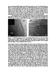
New method of reducing threading dislocation in epitaxial ZnO films grown on c-sapphire Yuekui Sun, and David Cherns Department of Physics, University of Bristol, H.H.Wills Physics Laboratory, University of Bristol, Tyndall Avenue, Bristol, BS8 1TL, United Kingdom ABSTRACT The behavior of threading dislocations (TDs) in ZnO/(0001)sapphire heterostructures grown by a two-step method have been investigated. The initial template, grown by pulsed laser deposition, consisted of a continuous underlayer, which was O-polar and an overlayer comprising a high density of Zn-polar nanorods. High densities (~7×1010 cm-2) of TDs were found to be restricted to the underlayer, whereas the nanorods were almost defect-free. Subsequent treatments by either hydrothermal growth or chemical vapour deposition (CVD) achieved epitaxial lateral overgrowth of nanorods and led to continuous Zn-polar films. The low TD density of nanorods remained until misoriented grain boundaries and boundary dislocations were generated when neighbouring nanorods become coalesced. The lateral migration of TDs in the overgrowth led to dislocation interactions and reduction of TDs. The total TD density at the top of the overlayer was estimated to be ~1×109 cm-2 for hydrothermal growth and ~7×109 cm-2 for CVD growth. INTRODUCTION Due to its wide band-gap (3.3 eV) and large exciton binding energy (60 meV), ZnO is a potential competitor to GaN for light emitting devices. ZnO has more immediate application in unipolar electronic devices where its high breakdown field, high saturation velocity and radiation hardness are very attractive [1], although its applications to bipolar light emitting diodes and laser diodes are still limited by difficulties in p-doping at present. Compared to GaN, the low growth and processing temperatures make ZnO very attractive for minimising costs and for growth on low melting point substrates, notably in organic electronics [2, 3]. The growth of an epitaxial layer with low densities of threading dislocations (TDs) on cheap, large area substrates is one of the keys to successful optical and electronic devices based on both ZnO and GaN materials. (0001) sapphire has been successfully applied for GaN based devices. There has also been extensive research to investigate the epitaxial growth of ZnO on (0001) sapphire because ZnO and GaN indeed have the same structure (hexagonal wurtzite). Among various growth methods, the epitaxial relationship, i.e. (0001)ZnO//(0001)sapphire with [11-20]ZnO//[10-10]sapphire, was found to be dominant [4, 5]. This gave an in-plane mismatch of 18.4% ([11-20]ZnO = 0. 974 nm, [10-10]sapphire = 0.824 nm), and an out-of-plane mismatch of 20% ([0001]ZnO = 0.5213nm, 1/2[0001]sapphire = 0.649 nm). Such high mismatch has resulted in high TD density, typically 109-1011 cm-2 [6-8]. Epitaxial lateral overgrowth (ELO) which has been proved to be an efficient way to reduce TDs in GaN epitaxial layers [9], has also been applied in ZnO growth. Using (111)MgAl2O4 as substrates, Andeen et al [10] deposited ZnO by hy
Data Loading...


