Evolution of tensile residual stress in thin metal films during energetic particle deposition
- PDF / 189,204 Bytes
- 4 Pages / 612 x 792 pts (letter) Page_size
- 29 Downloads / 322 Views
MATERIALS RESEARCH
Welcome
Comments
Help
Evolution of tensile residual stress in thin metal films during energetic particle deposition A. Misra and M. Nastasi Materials Science and Technology Division, Los Alamos National Laboratory, Los Alamos, New Mexico 87545 (Received 28 May 1999; accepted 21 September 1999)
Physical-vapor-deposited thin metal films often exhibit tensile residual stresses. We studied the stress evolution in thin Cr films and found that increasing bombardment with energetic particles (atoms or ions) at low energies leads to an increase of tensile stress to a maximum followed by a rapid decrease. Microstructural characterization by transmission electron microscopy revealed that two different microstructures are observed for the same level of tensile stress: films processed at low bombardment had columnar porosity while no porosity was observed in films processed at higher bombardment. The observed stress evolution is interpreted by considering how the mean interatomic distance (and hence the force) in the intercolumnar regions is modified by energetic particle bombardment.
Residual stresses are ubiquitous in polycrystalline physical-vapor-deposited (PVD) thin metal films, especially for deposition at low homologous temperatures.1–3 For nonenergetic deposition, such as slow evaporation or sputtering at high inert gas pressure, usually tensile stresses are observed.1– 4 The evolution of stress with film thickness for ambient temperature deposition has been found to fall into two classes.5 Type I behavior, observed in high melting point metals such as Cr, is characterized by large (>1 GPa) tensile stresses that reach a peak at thickness ∼4.5 Å significant interatomic attractive interaction is not expected. In this range of interatomic distances where tensile stress is observed, 1 > a/a0 艋 ∼1.5, how does one obtain quantitative estimate of stress? As shown in Fig. 3(b), the peak tensile stress from interatomic potentials is ∼28 GPa, while the experimentally observed peak stresses are ∼1.5 GPa. Using the model shown in Fig. 4, it follows that only a small fraction of atoms are located in the intercolumnar regions and experience high stresses; other atoms (e.g., in the center of the column) may experience no stress. Hence, the overall stress can only be obtained by averaging the interatomic forces in the plane of the film. As a simple example, let us assume that only the first layer of atoms on either side of the columnar void experiences the high 28 GPa stress and other atoms are stress-free. For a0 ≈ 2.9 Å and in-plane grain size of ∼160 Å, approximately 55 atom layers occupy the entire width of the column. If 2 atom layers experience stress, the fraction of atoms under the high stress is only ∼0.036. Hence, if the remaining atoms do not experience any
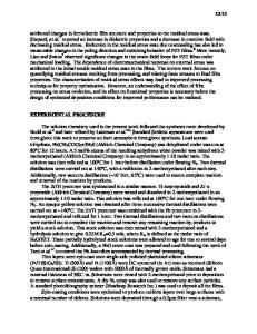
FIG. 4. Schematic of the columnar microstructure of the sputtered films studied showing how the interatomic attractive interaction between planar surfaces of adjoining columns can lead to elastic tensile straining. If the magnitude of the elasti
Data Loading...