Morphology Evolution of Pyramid-Like Nanostructures on Cobalt Thin Films During Deposition by Sputtering
- PDF / 427,156 Bytes
- 6 Pages / 595 x 842 pts (A4) Page_size
- 79 Downloads / 268 Views
H4.9.1
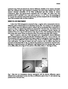
Morphology Evolution of Pyramid-like Nanostructures on Cobalt Thin Films during Deposition by Sputtering 1 1 Shih-Wei Chen , Jin-Ruey Wen , Chuan-Pu Liu1 and Jiun-Nan Chen2 1 Department of Materials Science and Engineering, National Cheng-Kung University, Tainan, Taiwan 2 Department of Electrical Engineering, Fortune Institute of Technology, Kaohsiung, Taiwan ABSTRACT The cobalt thin films are grown by D.C. magnetron sputtering as a function of the target-to-substrate distance, bias and power on both Si (100) and (111) substrates. The crystal structure and morphology of the thin films are characterized by 4-point probe, x-ray diffraction, scanning electron microscopy, transmission electron microscopy and atomic force microscopy. It is found that the cobalt crystal structure can be varied from HCP to FCC by varying the target–to-substrate distance from 6 to 10 cm. The resistivity, roughness and the preferred orientation of the thin films are greatly affected by the substrate bias and power. The lowest resistivity of Co films is 9.8 μΩ-cm when deposited at the target–to-substrate distance of 6cm, the applied power of 50W and the substrate bias of -75 volts. In addition, pyramid-like nanostructures with sharp tips are formed on the surface of the thin films when negative bias is applied. The faceted planes on the nanostructures depend on the resulting Co crystal structure while the size and density are determined by the growth parameters. The evolution of the surface nanostructures are systematically examined as a function of substrate bias and thin film thickness. The formation mechanism of the surface nanostructures is discussed in the paper. INTRODUCTION Cobalt possesses many superior properties including their electrical and magnetic properties and hence has attracted much attention [1,2]. For instance, cobalt has been successfully employ as catalyst for carbon nanotube (CNT) growth [3] and cobalt silicide has been investigated to replace titanium silicide in IC technology due to its thermal stability and lower resistivity [4]. Here we present the cobalt thin film growth by DC magnetron sputtering and show the microstructure evolution with various processing parameters. In addition, the pyramid-like nanostructures are found to form on cobalt thin film surface only under certain growth condition. The pyramid-like nanostructures has well defined shape and size with a sharp tip. The nanostructures might be applied in magnetic recording media or to grow CNT on its tip as the most active catalytic site. Therefore, we also investigate the nanostructure evolution with various processing parameters in great detail in this study. EXPERIMENTAL DETAILS A DC magnetron sputter is employed to deposit Co thin films on n-type Si(100) and (111) substrates. The substrates were chemically cleaned before loading into the chamber. The Co target (99.95% purity) is pre-sputtered for 10 minutes after base pressure of 3×10⁻⁶ torr is reached using argon (99.995% purity) as the sputtering gas. During deposition, the total gas flow an
Data Loading...