Evolution of the Surface Structure of CVD Tungsten During Annealing
- PDF / 2,307,381 Bytes
- 6 Pages / 414.72 x 648 pts Page_size
- 42 Downloads / 364 Views
(a) 1.5
I
1!
1 N
cn *~ 0.5 0 No etch or anneal
tW1O min.
0 6
II
7
I
8
9
Current (Amps)
10
11
(b)
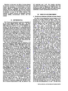
Figure 1: A scanning electron micrograph of the CVD deposit on a tungsten ribbon. The tungsten was deposited at a ribbon current of 8 amps for 10 minutes. (b.) The grain size plotted as a function of the specimen current during deposition. The time of deposition was 10 minutes.
22
WF 6 +3H2
-> W+6HF
(1)
The deposition was carried out by heating the tungsten ribbon in the tungsten hexafluoride vapor. The reaction then proceeds on the hot ribbon surface. During the deposition we could not measure the temperature of the ribbon directly, so we will report the deposition conditions in terms of the specimen current. The tungsten hexafluoride flow rate controlled the tungsten growth rate; i.e., the rate of WF 6 reaching the surface was less than the surface reaction rate limit of reaction 1. The hydrogen flow rate during the deposition was 2000 sscm; the hydrogen pressure was 1 torr. After preparation, the sample was resistively heated in a separate chamber to allow the surface structure to evolve. The heating was carried out with the sample in a small quartz bell jar; forming gas was flowing through the bell jar during the heating experiment. The temperature during heating was measured with a two-color optical pyrometer. The surface of the sample was analyzed in a variety of ways. Scanning electron microscopy was performed on all of the samples both before and after heating. This information gave an overall picture of the morphology of the sample and the size of the deposited grains. The grain size was measured with a linear intercept method using multiple photographs of the surface taken in the scanning electron microscope. More quantitative data about the surface roughness was obtained using atomic force microscopy. The instrument used for this study was a Park Scientific Scanning Force Microprobe. The two parameters that were found useful in describing the surface were the RMS roughness of the surface and the wavelength of this roughness. RESULTS The Structure of As-Deposited Material Figure la shows a scanning electron micrograph of CVD tungsten. The deposition conditions were a specimen current of 8 amps for a time of ten minutes. One can observe the hillocks on the surface with small gaps between them. It appears that each hillock represents a single grain that has nucleated on the surface of the ribbon. The grain size of these samples is plotted in Figure l b. There is a minimum in the grain size at specimen currents of 7.5 to 8 amps. There did not appear to be a significant difference in the morphology of the hillocks in samples heated between 7 and 9 amps. However, when the specimen current was twelve amps, the surface appeared to be flat. This result suggests that at this current the sample temperature was high enough that the hillocks were smoothed out as they were deposited. Much more information about these structures could be obtained by using the atomic force microscope (AFM). Figure 2 sho
Data Loading...