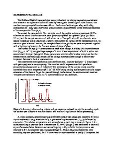
Effects of annealing on the structure and electrical conductivity of CVD alumina films
- PDF / 6,671,241 Bytes
- 8 Pages / 593.28 x 841.68 pts Page_size
- 79 Downloads / 356 Views
P.W. Cheung Department ofElectrical Engineering, University of Washington, Seattle, Washington 98195 (Received 9 September 1987; accepted 20 May 1988) Alumina films, 160 nm thick, were deposited on (100) -oriented silicon single-crystal substrates by pyrohydrolysis of aluminum chloride. Such films are candidate gate materials for an improvedpH ion-sensitivefield-effecttransistor ( / J H - I S F E T ) for industrial and medicalpH measurements. The current-voltage (I-V) characteristics of films annealed for 30 min at temperatures of 850,1000, and 1175 °C were determined. Annealing at 850 °C produced the optimum /- V behavior for the aluminum oxide/?H-sensitive films as evidenced by minimum leakage current and maximum breakdown voltage. The structures of the annealed films were examined using transmission electron microscopy. The anneals at 1000 and 1175 °C caused partial and complete transformation, respectively, of the as-deposited y-alumina to the aalumina phase. Associated with a-alumina formation was the creation of voids along the grain boundaries and in the grain interiors that provided paths of increased electrical conduction through the alumina films and degraded their dielectric behavior.
I. INTRODUCTION Understanding the relationship between the electrical properties and the microstructure of chemical-vapor-deposited (CVD) aluminum oxide thin films is required to fully optimize their utilization in advanced solid-state pH sensors. The present study was prompted by the desire to use the/>H-sensitive dielectric properties of aluminum oxide integrated with a field-effect transistor to create an improved ion-sensitive field-effect transistor (ISFET) I>2 as an advanced solid-state sensor. Such a sensor would be of great value in response to the long-standing demand for miniaturized sensors for process control and monitoring in various medical and industrial applications. An ISFET is conceptually similar to a field-effect transistor (FET), except that the metal gate is replaced by a solution gate.3"5 The solution gate is comprised of a dielectric material in contact with an electrolyte. The gate dielectric material develops a double-layer surface potential in response to the concentration of the potential determining ion (PDI) in the electrolyte.6"9 Aluminum oxide has been shown to possess amphoteric properties and to develop a surface potential when exposed to hydronium and hydroxyl ions. 10~12 Thus, aluminum oxide is a candidate material for the solution gate of apHsensitive ISFET. a> w
Now at Gould Inc., Foil Division, Eastlake, Ohio 44094. Now at NASA Lewis Research Center, Cleveland, Ohio 44135.
1002
J. Mater. Res. 3 (5), Sep/Oct 1988
http://journals.cambridge.org
The optimum gate dielectric material for a/>H-sensitive ISFET will not only exhibit a surface potential when exposed to both hydronium and hydroxyl ions,13 i.e., an amphoteric oxide, but must have good dielectric properties and be stable in the electrolyte environment. Aluminum oxide is an amphoteric oxide, generally very stable in most envir
Data Loading...