Excimer Laser Crystallization of Sputter Deposited a-Si Films on Flexible Substrates
- PDF / 826,726 Bytes
- 6 Pages / 612 x 792 pts (letter) Page_size
- 40 Downloads / 329 Views
I7.5.1
Excimer Laser Crystallization of Sputter Deposited a-Si Films on Flexible Substrates Yong Hoon Kim, Sung Kyu Park, Dae Gyu Moon, Won Keun Kim and Jeong In Han Information Display Research Center, Korea Electronics Technology Institute, Pyungtaek, Kyunggi, Korea.
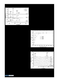
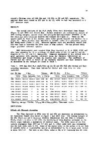
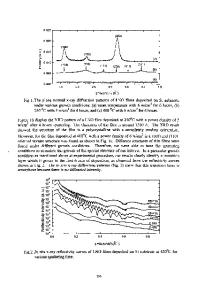
ABSTRACT In this report, excimer laser annealed polycrystalline silicon (poly-Si) films on flexible polymer substrates are investigated. The amorphous silicon (a-Si) films were first deposited on polycarbonate (PC) and polyethersulfone (PES) substrates by radio-frequency (RF) magnetron sputter and sequentially annealed by XeCl excimer laser annealing system (λ = 308 nm). The argon concentration of a-Si films which was estimated by Rutherford Backscattering Spectrometry (RBS) was found to be dependent on the dynamic pressure during the deposition process and the sputtering gas. Typically, the argon concentration of a-Si film was 1 ~ 2% when the film was deposited using argon gas at 6 mTorr. After the annealing process, the average grain size of the poly-Si film annealed with laser energy density of 289 mJ/cm2 was 400 nm estimated from transmission electron microscope (TEM) investigations.
INTRODUCTION Flexible display has been one of the most vital issues in display industries during the past decade due to its potential advantages such as light-weight, compactness, robustness and most of all, vast mechanical and design flexibilities compared to the conventional glass-based displays. These flexibilities will open a new era in display technology. A rollable display, wearable display and displays with various shapes will become reality using this technology. At an early stage of the development, simple passive-matrix liquid crystal displays (LCDs) using twisted nematic, super twisted nematic or ferroelectric liquid crystals have been intensively studied, which are mostly developed for small size mobile phones, smartcards and personal digital assistant (PDA) devices [1, 2]. However in order to satisfy the growing demands of multicolor, high definition and high performance displays, recent works mainly focus on the active-matrix flexible displays using amorphous silicon (a-Si) or low temperature polycrystalline silicon (LTPS) thin film transistors (TFTs) and they have been successfully demonstrated by a number of major flat-panel display manufacturers [3, 4]. In a-Si based TFT technology, plasma-enhanced chemical vapor deposition (PECVD) is mostly used in the deposition process of hydrogenated amorphous silicon (a-Si:H), doped a-Si and silicon nitride (SiNx) layers because relatively high quality films are obtained by PECVD method. In LTPS technology, there are several ways to fabricate polycrystalline films from amorphous films. Metal-induced crystallization (MIC) or metal-induced lateral crystallization (MILC) and excimer laser crystallization (ELC) are the most widely used processes [5-7]. In MIC method, the process temperature can be decreased to 350°C using field-enhanced (FE) technique [8]. However, the process temperature is still high for polymer
Data Loading...