Excimer Laser Induced Crystallization of Amorphous Silicon-Germanium Films
- PDF / 1,164,863 Bytes
- 6 Pages / 414.72 x 648 pts Page_size
- 8 Downloads / 390 Views
Physics Dept. ,Oregon Graduate Institute OR-97291-1000 Stanford University, Stanford,CA-94305 du Loess,F-67037 Strasbourg, France
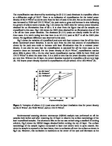
ABSTRACT Application of excimer laser crystallization of amorphous silicon (a-Si) has introduced a new, interesting potential technology for the fabrication of polycrystalline (poly-Si) thin film transistors. We are currently studying polycrystalline SilxGex thin films in order to determine whether this material can lead to improved electrical properties or to better processing requirements when compared with polycrystalline Si films. In this work we analyze by RBS , TEM , Raman spectroscopy and surface reflectance, the structure of thin amorphous Si 1-xGex films after irradiation with a XeCl excimer laser. The amorphous SiGe films were prepared by evaporation of Si and Ge onto oxidized Si substrates using an electron gun in vaccum .The effects of laser energy fluence during irradiation are investigated. The amorphous to crystalline transition is followed by in-situ measurement of time-resolved reflectivity. INTRODUCTION The use of lasers for the crystallization of amorphous silicon thin films has been investigated extensively in order to fabricate polycrystalline silicon thin film transistors (poly-Si TFrs) [1,6]. Due to the high absorption of UV-light in amorphous silicon, it is possible to melt the silicon at a very short time (nanoseconds) using a pulsed laser. The crystallization of the molten layer starts from the underlying substrate with a very high solid-liquid interface velocity typically of several meters per second. Since the laser energy is confined within a very small layer, this process can be executed without damage to the underlying glass substrate thereby allowing the use of low cost substrate materials.This process presents the unique advantage of permiting selective local crystallization methods to integrate , on the same glass substrate, both the high mobility poly-Si TFTs for the peripheral circuits and the low-mobility pixel addressing a-Si TFTs [7]. To date, poly-Si TFTs having mobilities higher than 300 cm 2 /V s were recently obtained by Zhang et al. [8] using a XeCI excimer laser. They were obtained by controlling the amount of impurities in the as-deposited films, by optimizing the laser parameters (laser energy density, number of shots and substrate temperature) and by using thin a-Si films of 50nm in thickness. On the other hand, King. et al. [9] have recently shown that polycrystalline silicongermanium (poly-SiGe) films with Ge fractions up to 0.6 are completely compatible with standard VLSI fabrication processes. They also observe an enhancement in the carrier mobility as a function of Ge content in the film. In addition, poly-Si lxGex is reported to be an attractive alternative to poly-Si in technologies like TFTs with limited thermal budget allowances [10,11]. This low-temperature processing capability, along with potential enhancement in carrier mobilities [9] have motivated us to investigate the formation and properties of poly-Si l-xGex films using e
Data Loading...