Experimental Limits of Light Capture in Thin Film Silicon Devices
- PDF / 836,255 Bytes
- 12 Pages / 612 x 792 pts (letter) Page_size
- 41 Downloads / 319 Views
1101-KK02-03
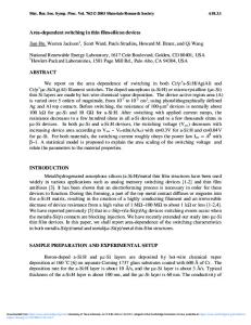
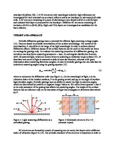
Experimental Limits of Light Capture in Thin Film Silicon Devices Ales Poruba1,2, Petr Klapetek3, Jakub Holovsky1, Adam Purkrt1, and Milan Vanecek1 1 Department of optical crystals, Institute of Physics, Academy of Sciences of the Czech Republic, Cukrovarnicka 10, Prague, 162 53, Czech Republic 2 Solartec s.r.o., Televizni 2618, Roznov pod Radhostem, 756 61, Czech Republic 3 Czech Metrology Institute, Okruzni 31, Brno, 638 00, Czech Republic ABSTRACT New approach for the determination of the angular distribution of the scattered light at nano-rough surfaces/interfaces from AFM (Atomic Force Microscopy) data is presented. Calculation comes from modeling the electromagnetic field in the tight vicinity of the nanorough surface by complex solution of Maxwell’s equations and subsequent near field to far field transform. This method is demonstrated for four types of transparent conductive oxides (with rough free surfaces) deposited on glass substrates. As a result we have the amount and angular distribution of the scattered light „observed” in both transmission and reflection. Moreover calculation can be done for real sample dimensions (to compare the results with the measurement of the angular distribution function using LED laser) or for a semi-infinite sample which suppresses the interference effects and thus such distribution functions can be used as an input parameter for our 3-dimensional optical model CELL for thin film silicon solar cell modeling. In the second part of this contribution we describe our experiment of thin film silicon solar cell characterization by Light Beam Induced Current (LBIC). This measurement done for laboratory solar cell structures reveals the light scattering and light trapping properties of the multilayer stack on a glass substrate. We suggest the test structure for the direct back reflector quality comparison and thus also for its optimization. INTRODUCTION Although the thin film silicon technology is now already mastered and it is becoming one of the most promising branches in a present photovoltaic industry there is still a room for their improvement. Optical, optoelectronic and electrical properties of all layers within the solar cell structure determine the resulting device performance. Therefore it is of great importance to have methods for particular material and final solar cell characterization as well as some modeling tool to be able to predict the structure behavior. Recently we have developed the 3-dimensional optical model CELL [1] for thin film silicon solar cells (amorphous, microcrystalline, single or multi-junction) with nano-rough surfaces/interfaces. For such cells the external quantum efficiency, short circuit current, total reflectance and all absorption losses can be computed taking into account roughness, angular distribution of scattered light, thicknesses and experimentally determined optical constants of all layers. The model can be used to simulate and/or compare the results with the experimentally determined measurements of real solar cells (T/R,
Data Loading...