Extended Quantum Model for Porous Silicon Formation
- PDF / 328,042 Bytes
- 6 Pages / 414.72 x 648 pts Page_size
- 108 Downloads / 403 Views
H. Miinder, St. Frohnhoff, M.G. Berger, M. Marso, M. Th~nissen, Rt. Arens-Fischer,H. Liith Institut fiir Schicht- und lonentechnik (1ST), Forschungszentrum Jiilich GmbH, D-52425 Jiilich, Germany
ABSTRACT The formation of porous silicon (PS) by electrochemical dissolution of bulk Si is described by a new model involving quantum mechanical calculations of the tunneling probability of holes through small crystallites (< 60 A) into the electrolyte. This tunneling probability shows oscillations as a function of crystallite size. The presented model calculations are in agreement to the microstructure of p-PS -- deduced from Raman measurements -- as a function of etching parameters and substrate doping level.
INTRODUCTION It has been known for nearly 40 years that porous Si (PS) can be formed by an electrochemical etch process [1]. During the last decades several models have been developed to describe the mechanism which leads to the spongelike structure of PS. These models have to account for the fact that the microstructure of PS layers depends on the etch parameters as well as on the substrate doping. The common idea of all models is an electrochemical reaction which requires the presence of holes at the electrolyte/Si interface for the dissolution of Si. The remaining porous structure is passivated against further dissolution by a depletion of holes in the PS layer. In the model proposed by Beale et al. [2, 3, 4] it has been assumed that a space charge region exists. The corresponding electric field lines are focussed at the pore bottom. Therefore, holes do not penetrate into the PS layer. In the quantum model the depletion of holes in the porous layer is due to the band offset at the PS/substrate interface [5]. Another well known model is the so called diffusion limited model [6]. Within this model the formation of PS is described by the diffusion of holes as a stochastic process. None of these models can describe all experimental results reported in literature. For example the different microstructures of PS formed on p-- and p+-doped substrates can not be explained within the diffusion limited model. In addition, the non-uniform size distribution functions found by Raman for all porosities and doping levels cannot be explained within any of these models [7]. In this paper experimental results and model calculations are reported which show that the quantum mechanical tunneling probability of holes through small crystallites into the electrolyte influences the microstructure of PS.
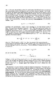
THEORY Similar to the quantum model it is assumed that the dissolution of Si can be described by an electrochemical etch process involving holes. The nanocrystallites formed during the etching process are passivated against further dissolution by the depletion of holes. This 315 Mat. Roes. Soc. Symp. Proc. Vol. 358 0 1995 Materials Research Society
electrolyte lPS I p - Si
U0
................. EF I- I__IVo - Ev
----- Ep N -------------Tj -
U>O X .0
1 L
0
Eh
Figure 1: Simplified band structure of the electrolyte/PS/substrate sy
Data Loading...