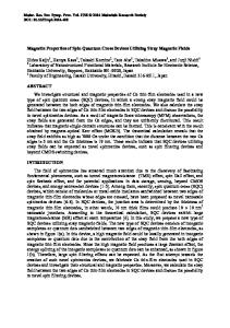
Fabrication and Current-Voltage Characteristics of Ni Spin Quantum Cross Devices with P3HT:PCBM Organic Materials
- PDF / 3,501,772 Bytes
- 6 Pages / 612 x 792 pts (letter) Page_size
- 28 Downloads / 244 Views
1252-J02-08
Fabrication and Current-Voltage Characteristics of Ni Spin Quantum Cross Devices with P3HT:PCBM Organic Materials Hideo Kaiju1, 2, Kenji Kondo1, Nubla Basheer1, Nobuyoshi Kawaguchi1, Susanne White1, Akihiko Hirata3, Manabu Ishimaru3, Yoshihiko Hirotsu3, and Akira Ishibashi1 1 Laboratory of Quantum Electronics, Research Institute for Electronic Science, Hokkaido University, Sapporo 001-0020, Japan 2 PRESTO, Japan Science and Technology Agency, Saitama 332-0012, Japan 3 The Institute of Scientific and Industrial Research, Osaka University, Ibaraki, Osaka 567-0047, Japan ABSTRACT We have proposed spin quantum cross (SQC) devices, in which organic materials are sandwiched between two edges of magnetic thin films whose edges are crossed, towards the realization of novel beyond-CMOS switching devices. In SQC devices, nanometer-size junctions can be produced since the junction area is determined by the film thickness. In this study, we have fabricated Ni SQC devices with poly-3-hexylthiophene (P3HT): 6, 6-phenyl C61-butyric acid methyl ester (PCBM) organic materials and investigated the current-voltage (I-V) characteristics experimentally and theoretically. As a result of I-V measurements, ohmic I-V characteristics have been obtained at room temperature for Ni SQC devices with P3HT:PCBM organic materials, where the junction area is as small as 16 nm x 16 nm. This experimental result shows quantitative agreement with the theoretical calculation results performed within the framework of the Anderson model under the strong coupling limit. Our calculation also shows that a high on/off ratio beyond 10000:1 can be obtained in Ni SQC devices with P3HT:PCBM organic materials under the weak coupling condition.
INTRODUCTION Molecular electronics have stimulated considerable interest as a technology that may enable a next generation of high-density memory devices [1,2]. Especially, in International Technology Roadmap for Semiconductor (ITRS) 2009 edition, molecular memory devices have been expected as candidates for beyond-CMOS devices since they offer the possibility of nanometerscale components [3]. Recently, we have proposed spin quantum cross (SQC) devices, in which organic materials are sandwiched between two edges of magnetic thin films whose edges are crossed, towards the realization of novel beyond-CMOS switching devices [4-7]. In SQC devices, the area of the crossed section is determined by the film thickness, in other words 1-20 nm thick films could produce 1×1-20×20 nm2 nanoscale junctions. This method offers a way to overcome the feature size limit of conventional optical lithography and to realize switching devices with a high on/off ratio. Moreover, the resistance of the electrode can be reduced down to ~kΩ since the width of films can be easily controlled to the one as long as ~mm. This makes it possible to detect the resistance of the junction with high sensitivity and to be applied to high-frequency
devices. Thus, SQC devices with organic materials can be expected as novel beyond-CMOS switching device
Data Loading...