Fabrication of Nanotips and Microbeams in Antimonide Based Semiconductor Material using Bromine Ion Beam Assisted Etchin
- PDF / 4,567,816 Bytes
- 6 Pages / 612 x 792 pts (letter) Page_size
- 14 Downloads / 400 Views
R7.7.1
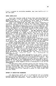
Fabrication of Nanotips and Microbeams in Antimonide Based Semiconductor Material using Bromine Ion Beam Assisted Etching B. Krejca1, S.R. Vangala1, K. Krishnaswami1, R. Kolluru1, M. C. Ospina2, C. Sung2 and W. D. Goodhue1 1. Photonics Center, Dept. of Physics, University of Massachusetts, Lowell, MA 01854 2. Center for Advanced Materials, University of Massachusetts, Lowell, MA 01854 ABSTRACT Antimonide-based compound semiconductors have emerged as the materials of choice for fabricating high-speed low-power electronics and electro-optics for applications requiring miniaturization and portability. In this work Br-IBAE is shown to be an anisotropic antimonide etching technique that is capable of generating novel structures as well as performing standard etching tasks. When etching less than optimally chemical-mechanical polished (111) InSb wafers, sharp-tipped cone structures with tip radii of the order of less than 60 nm are produced. These structures may be ideally suited for the development of field-emission devices, where small tip radii are required for useful emission currents. The anisotropic nature of the IBAE technique allows one to etch channels in the surface at angles up to 70º from perpendicular, making the fabrication of microbeams feasible. Using an angled sample holder, the first etch undercuts the masked beams from one side. The sample is then removed and realigned so as to undercut the beams from the other side. The triangular shaped microbeams are left suspended from either one or both ends. Using a combination of atomic force microscopy and mechanical engineering beam analysis techniques, the elastic parameters of the material can be measured. The microbeams can be aligned along various directions on the surface to investigate anisotropic characteristics. This is particularly important for determining the mechanical characteristics of materials that can only be grown in thin epitaxial layers, such as quaternary antimonide-based compound semiconductors. I.
Introduction
Antimonide-based compound semiconductors (ABCS) are now being used to fabricate high-speed low-power electronics and optoelectronic devices1. Recently, a number of GaSbbased photonic devices have been reported in the literature2,3,4. In fact, the ternary and quaternary antimonides, with quantum engineerable narrow bandgaps and high electron mobilities, are ideal candidates for such devices. Though interest in ABCS has increased lately, research into how to dry etch and subsequently fabricate these compounds into devices is still in its infancy as compared to other III-V based technologies, such as GaAs and InP. Low damage dry etching techniques such as gas cluster ion beam smoothing5 and chemical assisted ion beam etching6 have been proposed for preparing the surfaces and patterning antimonide-based materials instead of more traditional techniques such as wet etching7 and reactive ion etching. Here, we show Bromine-Ion Beam Assisted Etching (Br-IBAE) as an effective method for fabricating unique structures in ABCS material
Data Loading...