Fabrication of Silicon Nano-Crystal Dots on SiO 2 by Ultrahigh-Vacuum Chemical Vapor Deposition
- PDF / 256,883 Bytes
- 4 Pages / 612 x 792 pts (letter) Page_size
- 69 Downloads / 328 Views
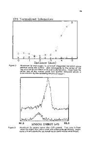
FABRICATION OF SILICON NANO-CRYSTAL DOTS ON SiO2 BY ULTRAHIGH-VACUUM CHEMICAL VAPOR DEPOSITION Masato Oishi, Takayuki Kawashima, Supika Mashiro, Junro Sakai, Sucharita Madhukar*, Bich-Yen Nguyen*, Bruce E. White*, ANELVA Corporation, Tokyo, Japan *Motorola Material and Structures Laboratories, Austin, TX ABSTRACT We report a process for Silicon (Si) nano-crystal dots fabrication using a cold-wall Ultrahigh-Vacuum Chemical Vapor Deposition (UHV-CVD) system. Si2H6 gas was used as the pre-curser and irradiated upon SiO2 film on Si wafer to form Si nano-crystal dots. In our system, nucleation, growth, and coalescence phases of nano-crystal dots on SiO2 were found to be related with the optical pyro-meter’s read-out curve. At first, the optimum gas irradiation time which gives the highest dot density without coalescence was decided for every gas irradiation condition by using an optical pyro-meter. Then, the dependence of optimum gas irradiation time, dot diameter and dot density on gas flow rate and wafer temperature were investigated. A decrease of wafer temperature or an increase of gas flow rate during the nucleation and growth phase results in a decrease of dot diameter and an increase of dot density. The optimum gas irradiation time was prolonged by decreasing wafer temperature or gas flow rate. Finally, a reproducible process of forming non-coalesced, small size, and high-density Si nano-crystal dots of about 5.5nm in diameter with density of 1x10¹² dots/cm2 were obtained. Typical process time to get such dot formation characteristics was about 10 minutes, which were long enough for ensuring reproducibility. INTRODUCTION Recently, a lot of researches have been made as for application of the Si nano-crystal dots to Flash Memories [1,2]. In those researches, Si nano-crystal dots embedded within gate dielectric were used as discrete charge storage elements in flash memory, which conventionally had continuous polycrystalline Si film as floating gates. By using Si dots, leakage current through the tunnel oxide can be drastically reduced with thinner oxide thickness, which makes lower programming voltage feasible. In such flash memories, density and size of Si dots closely relate to device characteristics such as Vth, therefore, precise control of Si nucleation process should be achieved. Conventional LPCVD system with typical process time of nucleation less than half a minute [3], can have difficulties in reproducibility of the process. Furthermore, it would also pose a new challenge to fabricate high-density (1x10¹²/cm2) and uniform-sized (5nm) dots, which are desirable for the next generation flash memory application. In this paper, we report a method for monitoring Si dots fabrication as well as the relationship between CVD parameters and dot morphologies in our cold-Wall UHV-CVD system. EXPERIMENT Figure1 shows the UHV-CVD system used in this study. The growth-chamber is made of stainless steel, which is suitable for realization of UHV background and for water-cooling of the chamber wall. The typical F6.4.1
Pyrom
Data Loading...