Fabrication of two-dimensional Si/Ge nanowires and nanorings
- PDF / 353,181 Bytes
- 5 Pages / 612 x 792 pts (letter) Page_size
- 59 Downloads / 367 Views
T1.7.1
Fabrication of two-dimensional Si/Ge nanowires and nanorings
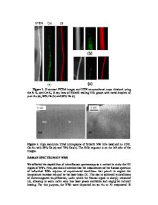
Midori Kawamura1,2, Bert Voigtländer1, Neelima Paul1, and Vasily Cherepanov1 1 Institut für Schichten und Grenzflächen, ISG 3, Forschungszentrum Jülich, 52425 Jülich, Germany 2 The present address: Kitami Institute of Technology, Department of Materials Science, Kitami, 090-8507 Japan ABSTRACT We show that two-dimensional Si/Ge nanostructures with a thickness of a single atomic layer can be imaged with chemical sensitivity using a scanning tunneling microscope (STM). An atomic layer of Bi terminating the surface is used to distinguish between Si and Ge. This distinction between Si and Ge enabled us to fabricate two-dimensional Si/Ge nanostructures in a controlled way by self-organized growth. Si/Ge nanoring structures consisting of alternating Si and Ge rings having a width of ~5 nm were grown around a Si core on a Si(111) substrate by molecular beam epitaxy (MBE). The thickness of the Si and Ge rings is only one atomic layer (0.3 nm). Alternating Si/Ge nanowires with a width of ~3.5 nm and a thickness of 0.3 nm were also fabricated using alternating Si/Ge deposition in the step flow growth mode. INTRODUCTION Recently great attention has been paid to nanostructured materials for the purpose of scientific interests and application to nanoelectronic devices. Semiconductor nanowires, for example, have a possible application as nanosized interconnects; quantum dots are also investigated intensively. Ge/Si heteroepitaxy has been widely studied as a model system for fundamental study of semiconductor heteroepitaxy [1]. Fabrication of nanostructures by molecular beam epitaxy (MBE) followed by structure analysis using STM is one of the conventional methods for the study of nanosized structures. However, it has been difficult to distinguish between the elements Si and Ge in thin films and especially in two-dimensional structures at surfaces except under selected conditions [2,3]. We have found a new distinction method of imaging two-dimensional Si/Ge nanostructures, with chemical sensitivity using an STM [4]. We use an atomic layer of Bi for termination of the nanostructures. It turns out that the apparent height measured by the STM is ~ 0.08 nm higher at areas consisting of Ge than on areas consisting of Si. This distinction enables us to investigate whether Ge and Si atoms intermix at
T1.7.2
the surface or not and we are able to find better deposition conditions for the fabrication of Si/Ge derived nanostructures. In the present paper, we report on examples of nanostructures consisting of alternating Si and Ge nanorings and nanowires. EXPERIMENTAL A solid-source MBE apparatus containing a Bi Knudsen cell, Ge, Si evaporators and a home built beetle type STM were used for the fabrication and analysis of the nano structures. The substrate temperature was monitored with an infrared pyrometer. Deposition rate was measured before each deposition using a quartz crystal microbalance (QCM) and/or electron impact emission spectroscopy (EIES) which is known for
Data Loading...