Fabrication of ZnO Bridging Nanowire Device by a Single-Step Chemical Vapor Deposition Method
- PDF / 780,262 Bytes
- 7 Pages / 612 x 792 pts (letter) Page_size
- 107 Downloads / 392 Views
1144-LL17-03
Fabrication of ZnO Bridging Nanowire Device by a Single-Step Chemical Vapor Deposition Method Yanbo Li, Ippei Nagatomo, Ryohei Uchino, Ichiro Yamada, and Jean-Jacques Delaunay Department of Engineering Synthesis, The University of Tokyo, 7-3-1 Hongo, Bunkyo-ku, Tokyo 113-8656, Japan
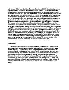
ABSTRACT ZnO nanowires are directly integrated into a working device by a single-step chemical vapor deposition (CVD) method. Gold catalyst is patterned on a quartz glass substrate using a comb-shaped shadow mask and then ZnO is grown on the patterned substrate by CVD. Thick ZnO layers formed on the gold-patterned areas serve as native electrodes. Ultra-long (~100 µm) ZnO nanowires grown across the gap between the ZnO electrodes and the nanowires serve as the sensing elements of the device. The device exhibits high sensitivity and fast response to UV illumination in air. Our method can be used to fabricate other metal oxide semiconductor bridging nanowire devices, which have promising applications in photodetection and gas sensing.
INTRODUCTION Zinc oxide is a direct, wide bandgap (Eg ~ 3.4 eV) semiconductor material with a wide range of properties from UV detection to gas sensing [1-5]. The sensing properties of ZnO and other metal oxides are governed by the charge-exchange reactions with adsorbants on the surface [6]. Due to their inherently high surface-to-volume ratio, ZnO nanowires offer the promise of high sensitivity. Although the nanowires can be grown by simple thermal evaporation or chemical vapor deposition (CVD) methods with relatively low cost [7-9], the integration of the nanowires into working devices still remains a challenge. The integration of nanowires is usually done by “bottom-up” and then “top-down” processes. The nanowires are grown by “bottom-up” processes such as thermal evaporation or CVD. Then, they are collected from substrates and dispersed in a solution. After that, the nanowires are randomly deposited on an insulating substrate. The positions of the nanowires are noted under scanning electron microscope (SEM) observation with the assistance of pre-patterned markers on the substrates. Thereafter, metallic contacts to the nanowires are fabricated by “top-down” techniques such as photolithography [10], electron beam lithography [11], or focused ion beam lithography [12]. Because of its complexity, low efficiency and high cost, this method is limited to fundamental studies of properties of nanowires. In recent years, a new process has been developed to integrate nanowires into working devices. It is based on the concept of bridging nanowires between electrodes by self-organized growth of nanowires [13-19]. On contrary to the first method, the bridging method employs a “top-down” process to make the electrodes, and then uses a “bottomup” process to grow the nanowires. A single crystal substrate is usually used to make a trench
and form electrodes on both sides of the trench by a “top-down” process. Then, nanowires are grown across the trench from one electrode to the other, forming bridges dire
Data Loading...