Fabrication, Properties and Electrochemical Applications of Diamond Nanostructures
- PDF / 4,493,304 Bytes
- 12 Pages / 612 x 792 pts (letter) Page_size
- 22 Downloads / 433 Views
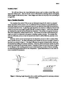
Fabrication, Properties and Electrochemical Applications of Diamond Nanostructures Nianjun Yang*, Waldemar Smirnov, Christoph E. Nebel Fraunhofer-Institute for Applied Solid State Physics (IAF) Tullastrasse 72 Freiburg 79108 Germany ABSTRACT We summarized in this paper the fabrication, properties, and electrochemical applications of diamond nanostructures, mainly diamond nanotextures and diamond nanowires. The characterizations of nanostructures were introduced with different techniques. As example of applications, electrochemical DNA sensing and protein trapping on diamond nanotextures are shown. INTRODUCTION Diamond, which is one of the promising wide-band gap semiconductors, has been considered as an excellent material for many applications due to its unusual chemical and physical properties.1-6 Much attention has thus been paid to its growth, characterization, applications, and devices realization.2-6 Depending on the type of doping, diamond can be n- or p-type conductive, resulting in a wide variation of conductivity from insulating, semiconducting, to metallic. Heavily boron-doped diamond films have been recognized as the best electrode materials for electrochemistry and biochemical applications. These diamond films have shown unique features such as i) high chemical stability in harsh environments, high current densities as working electrodes ii) weak or no surface bio-fouling; iii) biocompatibility; iv) low and stable capacitive currents in aqueous and organic solutions; and v) wide electrochemical potential window. For example, the capacitive current of a hydrogen terminated, boron-doped diamond electrode (boron concentration: 2×1020 cm-3) in 0.1 M pH 7 phosphate buffer is 10 times lower than that of a gold electrode and about 100 times lower than that of a glassy carbon electrode. A typical electrochemical potential window for diamond electrodes is 3.25 V in neutral and basic solutions.5 In organic solutions or ionic liquids, the electrochemical potential window of diamond is even wider. The diamond surface can be terminated with hydrogen, hydroxyl, and oxygen, which allows tuning the electronic properties of the solid/electrolyte interface with respect to energy alignments of interacting levels.1-3 These terminations can be achieved by plasma treatment at high temperature under different atmospheres1-3 or by electrochemical reduction/oxidation at high current densities in acid solutions.7 Moreover, it is ultra-hard (50-150 GaP).8 Diamond is thus a promising candidate for applications in different nanostructures. By creating diamond based nanostructures, it is possible to utilize the properties of diamond for applications which require strong mechanical stability in combination with chemical stability. These nanostructures are attractive especially for giant surface-to-volume ratio enhancements.9,10 The realization of diamond nanostructures started in 1997 by Shiomi,11 who demonstrated for the first time the formation of porous diamond films by reactive ion etching (RIE) using O2. Later in 2000, nanostruct
Data Loading...