FIB Precise Prototyping and Simulation
- PDF / 2,031,703 Bytes
- 13 Pages / 612 x 792 pts (letter) Page_size
- 74 Downloads / 362 Views
0960-N10-03-LL06-03
FIB Precise Prototyping and Simulation Philipp M. Nellen1, Victor Callegari1, Juergen Hofmann1, Elmar Platzgummer2, and Christof Klein2 1 Electronics/Metrology/Reliability, EMPA, Ueberlandstrasse 129, Duebendorf, CH-8600, Switzerland 2 IMS Nanofabrication GmbH, Schreygasse 3, Wien, A-1020, Austria
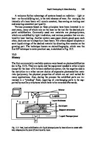
ABSTRACT We present a closed approach towards direct microstructuring and high precision prototyping with focused ion beams (FIB). The approach uses the simulation of the involved physical effects and the modeling of geometry/topography during milling while the ion beam is steered over the surface. Experimental examples are given including the milling of single spots, trenches, rectangles, and Fresnel lenses. Good agreements between simulations and experiments were obtained. The developed procedures can also be applied to other FIB prototyping examples. INTRODUCTION First applications of focused ion beam microscopes (FIB, typically Ga+, 20 – 50 kV) were chip modifications and repair, cross-sections, and TEM-lamella for characterization of devices and materials. Nowadays one scientific challenge amongst others is FIB micromachining, i.e., the fabrication of precise 3D surface structures with micrometer down to nanometer accuracy. The scanning ion beam allows structuring and modification of materials in three ways, first by direct sputtering, second by gas enhanced etching, and third by gas assisted material deposition. We will focus herein on structuring and simulation by direct sputtering. Direct sputtering does not require any lithography masks or multiple processing steps and is therefore an interesting tool for rapid prototyping and evaluation of structures. Typical sputter rates are between 0.1 µm3/nC (Cr, Al2O3) and 1.5 µm3/nC (Au) with most values around 0.27 µm3/nC (Si) [1, 2]. Sputtering is a relatively slow process. For example, milling of a volume of 10 x 10 x 10 µm3 in Si requires 1 h at an ion current of 1 nA. FIB micromachining is thus applied for feature sizes between 100 µm down to 10 nm which is the current limit of commercial FIBs due to their focus ability given by the current ion beam optics. However, patterning resolution below 5 nm was demonstrated recently [3]. Typical aspect ratios obtained are around 5:1 and with gas enhanced etching, where material is more easily removed, ratios of 15:1 are possible. However, due to beam skirts and beam overlapping sidewalls cannot be made perpendicular to the surface but have slopes around 85° instead of 90°. The principle to obtain the required precision for complex geometries is to adjust the ion fluence for each point of the structure separately. Depending on the degree of complexity the following three approaches can be made: “best-guesses”, experimental “trial-and-error”, or simulation programs. This paper discusses the principle of ion beam sample interaction as far as it is required to understand the following three aspects: simulations of ion matter interaction at energies up to 100 keV, simulation of topography evolution during direc
Data Loading...