Field emission from heterostructured nanoseeded diamond and nanocluster carbon cathodes
- PDF / 379,604 Bytes
- 5 Pages / 612 x 792 pts (letter) Page_size
- 86 Downloads / 365 Views
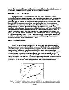
Field emission from heterostructured nanoseeded diamond and nanocluster carbon cathodes. B.S.Satyanarayana1*, K.Nishimura 2 , A.Hiraki 3 , W.I.Milne 1. 1 Electronic Devices & Materials Group,Engineering Dept, University of Cambridge, Cambridge .UK 2 KUT Academic & Industrial Collaboration Centre, Kochi University of Technology, Kochi, 782-8502, Japan. 3 Kochi Prefectural Industrial Tech. Center, 3992-3, Nunoshida, Kochi, 781-5101, Japan. ABSTRACT Novel heterostructured cold cathodes made of nanoseeded diamond and cathodic arc process grown nanocluster carbon films, were studied. The nanocrystalline diamond with varying diamond concentration was first coated on to the substrate. The nanocluster carbon films were then deposited on the nanoseeded diamond coated substrates using the cathodic arc process at room temperature. The resultant heterostructured microcathodes were observed to exhibit electron emission currents of 1µA/cm2 at low fields of 1.2 - 5 V/µm. Further some of the samples seem to exhibit I-V characteristics with a negative differential resistance region at room temperature conditions. This negative differential resistance or the resonant tunneling behaviour was observed to be dependent on the nanoseeded diamond concentration. INTRODUCTION There is an increasing interest in field assisted electron emission from carbon based nanostructured materials. Recently low field electron emission has been reported using many nanostructured materials including nanocrystalline diamond,[1-3] nanotubes[4,5] and nanocluster carbon[6-9]. The interest stems from the diverse applications such as electron-beam lithography, electron and ion guns, sensors, electron microscopes and microprobes, low & medium power compact microwave sources and Tera hz communication devices being envisaged for these electron emitters, besides field emission displays. The need is for electron emitters capable of emitting high emission currents at low fields accompanied by a high emission site density. Further the material and the growth process should be adaptable to varying application needs. Most of the low field electron emitters reported, have been grown using high temperature processes such as hot filament CVD, microwave plasma CVD, Plasma assisted DC discharge and cathodic arc process for nanotube growth.[1-5,8] Only the coral like carbon films[6] and the nanocluster carbon films [7] grown using the cathodic arc process have been deposited at room temperature. For a better idea, let us compare the electron emission from three different nanostructured carbon based materials. Figure-1 shows the current density against applied field plot for these different cathode materials. Figure 1 includes emission characteristics from a nanocluster carbon film grown using cathodic arc,[7] nano structured carbon films produced by supersonic carbon cluster beams generated by a pulsed plasma cluster source [9] and the nano-crystalline diamond films grown using the hot filament CVD [HFCVD].[3] It can be seen that all the samples exhibit electron emission curren
Data Loading...