Formation and stability of the prismatic stacking faultin wurtzite (Al, Ga, In) nitrides
- PDF / 154,340 Bytes
- 6 Pages / 612 x 792 pts (letter) Page_size
- 57 Downloads / 292 Views
CTION Extensive research effort is being undertaken on wide band gap of GaN based semiconductors for their very promising device possibilities. Efficient laser diodes have been fabricated for emission in the blue range[1] in layers grown on sapphire by Metal Organic Vapor Epitaxy (MOVPE). The active GaN layers contain large densities of crystallographic defects[2,3], among which, one finds {1 2 10} planar defects which have recently been called double positioning boundaries (DPBs)[4,5], stacking mismatch boundaries (SMBs)[6] or inversion domain boundaries (IDBs)[7]. These faults have recently been investigated using High Resolution Electron Microscopy (HREM) and Convergent Beam Electron Diffraction (CBED), and it was shown that they are stacking faults on top of both sapphire and SiC[8-10]. In fact these planar defects have already been studied in the sixties and two displacement vectors have been measured by conventional microscopy[11,12]. In wurtzite ZnS, Blank et al[12] were the first to study the planar defects which folded from basal to prismatic {1 2 10} planes, and to interpret them as stacking faults whereas other authors considered them to be thin lamella of the sphalerite phase in CdS[13]. In this work, we have investigated these faults in (Al,Ga)N epitaxial layers by HREM and
F99W3.55
modified the Stillinger-Weber[14] (SW) potential in order to analyze their stability in AlN, GaN, InN. The theoretical results were found to correlate with the HREM observations for AlN and GaN.
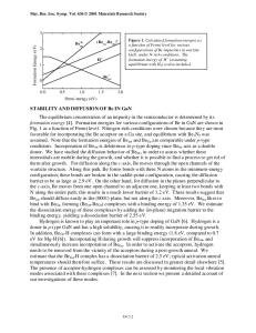
RESULTS The stacking fault atomic structure Two atomic models exist in the literature for the { 1120 } prismatic fault in wurtzite materials as originally characterized by conventional electron microscopy in the 60s by Drum[11] and Blank[12], respectively. Their projections are shown in figure 1 along [0001].
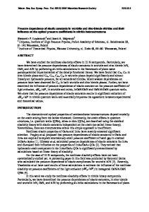
Figure 1. Atomic configurations of the { 1120 }stacking fault seen along [0001], a) The ½ [ 1011 ] displacement vector, b) The 1/6 [ 2023 ] stacking fault Formation mechanisms A. Formation on (0001) 6H-SiC surface The [0001] SiC surface exhibits steps of various heights. If one ignores the mismatch along the c axis which is small, the GaN and SiC can be geometrically considered as polytypes.
Figure 2. Generation of a prismatic stacking fault on a I1 type of step on the (0001) surface of 6H-SiC
F99W3.55
A 6H-portion under a step can be decomposed into a faulted 2H stacking, and depending on the type of step, the decomposition may result in a displacement vector between the two crystallites which grow on the adjacent terraces (fig.2). In fact between the two polytypes, the only displacement vectors d which can result from the decomposition are those of the hcp lattice ( the intrinsic I1, RI1 = 1/6 < 2023 >, I2 , RI2 = 1/3 < 1010 > and the extrinsic E, RE = 1/2 ). Among them, I1 and E have 1/2c component along the c axis and may lead to the formation of an extended defect in the epitaxial layer (fig.2). The displacement vector identical to I2 is confined in the interface and may contribute to release the misfit strain. When
Data Loading...