Formation of Nanovoids and Nanocolumns in High Dose Hydrogen Implanted ZnO Bulk Crystals
- PDF / 1,668,914 Bytes
- 6 Pages / 612 x 792 pts (letter) Page_size
- 53 Downloads / 326 Views
0957-K09-01
Formation of Nanovoids and Nanocolumns in High Dose Hydrogen Implanted ZnO Bulk Crystals R. Singh1, R. Scholz1, U. Gösele1, and S. H. Christiansen1,2 1 Max Planck Institute of Microstructure Physics, Weinberg 2, Halle, 06120, Germany 2 Physics Department, Martin-Luther-University Halle-Wittenberg, Hoher Weg 8, Halle, 06099, Germany
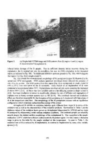
ABSTRACT ZnO(0001) bulk crystals were implanted by 100 keV H2+ ions with various doses in the range of 5×10¹⁶ to 3×1017 cm-2. The ZnO crystals implanted up to a dose of 2.2×1017 cm-2 did not show any surface exfoliation after post-implantation annealing at temperatures up to 800°C for 1 h while those crystals implanted with a dose of 2.8×1017 cm-2 or higher exhibited exfoliated surfaces already in the as-implanted state. In a narrow dose window in between, controlled exfoliation could be obtained upon post-implantation annealing. Cross-sectional transmission electron microscopy (XTEM) of the implanted ZnO wafers showed that a large number of nanovoids, having dimensions of about 10 nm, were formed within the implanted zone of ZnO. These nanovoids served as precursors for the formation of microcracks leading to the exfoliation of ZnO surfaces. In addition to the nanovoids, a number of nanocolumns perpendicular to the ZnO surface were also formed. These nanocolumns had diameters of up to 10 nm and lengths of up to 500 nm. The nanocolumns were found in the ZnO lattice well beyond the projected range of hydrogen ions. INTRODUCTION ZnO, a wide bandgap semiconductor having a large exciton binding energy of 60 meV, has currently been the subject of immense interest due to its potential applications in ultra-violet (UV) optoelectronic devices, transparent high power and high frequency electronic devices, surface acoustic devices and chemical gas sensors.1,2 It possesses a wurtzite crystal structure and is closely lattice-matched to GaN (about 2% lattice-mismatch). Hence, ZnO can potentially be used for the growth of high quality epitaxial layers of GaN and related nitrides.3,4 ZnO films are mostly grown epitaxially on lattice and thermally mismatched substrates such as sapphire, Si and SiC due to the fact that ZnO bulk substrates are very expensive and are mostly available in small sizes.5,6 The heteroepitaxial growth of ZnO on foreign substrates leads to the formation of growth-related defects such as dislocations, stacking faults and twins that occur to relax the strain.7 These defects in ZnO epilayers grown on hetero-substrates have deleterious effects on the performance and reliability of the devices fabricated utilising these layers. One of the promising methods to fabricate inexpensive and high structural quality substrates, comparable to bulk ZnO crystals, for the epitaxial growth of ZnO device layers would be direct wafer bonding and layer transfer of thin ZnO films onto inexpensive substrates via high dose hydrogen
implantation and layer splitting upon annealing.8,9 This process is based on the agglomeration of hydrogen implantation-induced platelets or nanovoids upon ann
Data Loading...