Frequency-Dependent Electromechanical Response in Ferroelectric Materials Measured via Piezoresponse Force Microscopy
- PDF / 371,225 Bytes
- 6 Pages / 595 x 842 pts (A4) Page_size
- 109 Downloads / 382 Views
C11.3.1
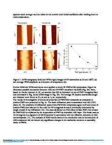
Frequency-Dependent Electromechanical Response in Ferroelectric Materials Measured via Piezoresponse Force Microscopy I. K. Bdikin, V. V. Shvartsman, S-H. Kim1, J. Manuel Herrero2, and A. L. Kholkin Department of Ceramics and Glass Engineering/CICECO, University of Aveiro, 3810-193 Aveiro, Portugal 1 INOSTEK Inc., Gyeonggi Technopark, 1271-11 Sa 1, Sangnok, Ansan, Gyeonggi 425-791, Korea 2 Instituto de Ciencia de Materiales de Madrid, CSIC, Cantoblanco, 28049 Madrid, Spain ABSTRACT Local piezoelectric signal is measured via Piezoresponse Force Microscopy (PFM) in PbZr0.3Ti0.7O3 films and PbZr1/3Nb2/3O3−0.045PbTiO3 single crystals. It is observed that the amplitude of piezoelectric response is almost independent on frequency for vertical (out of plane) signal and strongly decreases with increasing frequency in the range 10-100 kHz for lateral (in-plane) response. Moreover, the in-plane piezoelectric contrast is reversed when the measurements are done at high enough frequency (phase shift exceeds 90º). As a result, the inplane polarization direction can be misinterpreted if the driving frequency exceeds certain level. For the explanation of observed effect a simple model is proposed that takes into account a possible slip between the conductive PFM tip and moving piezoelectric surface. The implications of the observed frequency-dependent contrast for the domain imaging in ferroelectric materials are discussed. INTRODUCTION Ferroelectric domain imaging via scanning force microscopy (SFM) techniques is becoming a standard procedure for the investigation of ferroelectrics and related materials. Given its unprecedented resolution and flexibility, these techniques are now indispensable for the development of miniaturized electromechanical sensors and actuators, nonvolatile memory cells, nonlinear optical devices, etc [1]. Moreover, these techniques are likely to be used in the emerging area of ferroelectric domain engineering, where artificial domain patterns are created and stabilized in predetermined locations giving rise to an improvement of materials properties [2]. Another range of possible applications concerns with dense memory devices, where information bits are written and read by means of reorientation of ferroelectric domains via SFM tip [3]. It should be mentioned that this and other useful SFM functions could be achieved if the conducting SFM tip is in the direct contact with the investigated surface and imaging is performed via application of an ac voltage between the tip and the bottom electrode. In this case, the tip follows piezoelectric vibrations of the sample that are coupled to polarization and dielectric constant. This allows for the visualization of domain structure and, by applying dc voltages, for writing information bits by means of reversed domains. This technique called piezoresponse force microscopy (PFM) [4] has proved its significance in science and technology of ferroelectrics and piezoelectrics. One of the major advantages of PFM as compared to other techniques is the ability of a
Data Loading...