Piezoresponse Force Microscopy: A Window into Electromechanical Behavior at the Nanoscale
- PDF / 1,177,899 Bytes
- 10 Pages / 612 x 792 pts (letter) Page_size
- 38 Downloads / 312 Views
D.A. Bonnell, S.V. Kalinin, A.L. Kholkin, and A. Gruverman Abstract Piezoresponse force microscopy (PFM) is a powerful method widely used for nanoscale studies of the electromechanical coupling effect in various materials systems. Here, we review recent progress in this field that demonstrates great potential of PFM for the investigation of static and dynamic properties of ferroelectric domains, nanofabrication and lithography, local functional control, and structural imaging in a variety of inorganic and organic materials, including piezoelectrics, semiconductors, polymers, biomolecules, and biological systems. Future pathways for PFM application in high-density data storage, nanofabrication, and spectroscopy are discussed.
Introduction Over the last two decades, scanning probe microscopy has been instrumental in advancing our understanding of fundamental phenomena in many fields, including superconductivity, spin-resolved transport, charge density wave transitions, protein folding, chemical sensing, and catalysis. A particularly interesting case is piezoresponse force microscopy (PFM), which is unique in that it probes a tensorial property, the coupling between electric field and mechanical strain. While the first and most obvious application of this technique is to straightforwardly map domains in ferroelectric materials, PFM does much more both in terms of the information content and of applications. Coupling between electric fields and mechanical strain underpins a broader range of phenomena in ferroelectrics and other polar materials. 648
This article highlights recent examples in which PFM directly probes electromechanical interactions in systems ranging from complex ferroelectric materials and piezoelectric compounds to biological tissues. These examples also illustrate that creative variants of PFM or a quantitative approach to data analysis contribute to a fundamental understanding of complex phenomena in solids.
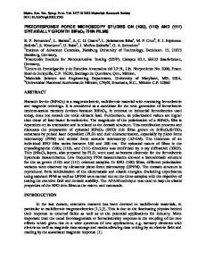
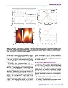
Imaging of Ferroelectric Domains: Statics and Dynamics PFM utilizes a basic experimental setup of atomic force microscopy in which a conducting tip at the end of a cantilever is brought in contact with a piezoelectric sample. When a voltage is applied to the tip, the resulting deformation of the sample is monitored through the mechanical displacement of the cantilever—piezoresponse.
While the concept is straightforward, quantification of properties can be complicated due to the complex sample-probe signal transfer mechanism. Nevertheless, considerable progress has been made in developing protocols for quantitative materials characterization with PFM.1 It is now routine to map ferroelectric domains based on variations of the amplitude and phase of the piezoresponse to the ac bias applied to the tip. PFM has been developed as an alternative to electron microscopy in the high-resolution imaging of ferroelectric domains in thin films, which in the case of PFM can be performed in a nondestructive manner. Further development of PFM has been stimulated by the need to understand the mechanism of the
Data Loading...