GaAs HEMT Reliability and Degradation Mechanisms after Long Term Stress Testing
- PDF / 298,065 Bytes
- 7 Pages / 612 x 792 pts (letter) Page_size
- 4 Downloads / 371 Views
1195-B05-04
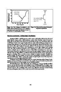
GaAs HEMT Reliability and Degradation Mechanisms after Long Term Stress Testing E. A. Douglas1, D. Cheney2, K. H. Chen3, C. Y. Chang1, L. C. Leu3, B. Gila1, F. Ren3, C. Abernathy1, S. J. Pearton1 1 Dept. of Materials Science and Engineering, University of Florida, Gainesville, Florida 32611 2 Dept. of Electrical and Computer Engineering, University of Florida, Gainesville, Florida 32611 3 Dept. of Chemical Engineering, University of Florida, Gainesville, Florida 32611 ABSTRACT GaAs based metamorphic and pseudomorphic high electron mobility transistors (HEMTs) under DC and thermal stress were studied. InAlAs/InGaAs MHEMTs grown on GaAs substrates were stressed at a drain voltage bias of 2.7V for 36 hours as well as thermally stressed at 250°C for 36 hours. Under both stress conditions, the drain current density decreased about 12.5%. The gate current, however, increased more after the thermal storage as opposed to DC bias. Reaction of the Ohmic contact with the underlying semiconductor was the main cause of degradation after thermal stressing. Transmission electron microscopy verified that gate sinking occurred in devices that underwent DC bias stressing. InGaAs pHEMTs that received a 1000 hour lifetime stress test from a commercial vendor showed similar degradation as virgin devices when stressed under DC bias for 24 hours. Virgin devices that were thermally stressed while undergoing DC bias showed minimal degradation up to 120°C, but exhibited catastrophic failure at 140°C. INTRODUCTION An assortment of degradation mechanisms have been identified in GaAs based high electron mobility transistors (HEMTs). These mechanisms range from contact degradation, electron and hole trapping/detrapping, corrosion, and fluorine contamination(1-18). Due to the commercial applications of metamorphic HEMTs (MHEMTs), such as low noise mm-wave amplifiers for radio communications and high bit-rate fiber systems, device reliability is of great concern(16) At 125°C, InP HEMTs exhibit a mean-time-to-failure (MTTF) of over 106 hours (17,18) . There is significant interest to develop GaAs MHEMTs because it is possible to grow on larger, less brittle wafers at a lower cost. Numerous studies have shown that InAlAs/InGaAs MHEMTs have a similar (MTTF) to InP HEMTs, though a burn-in step is required in order to improve device stability and remove devices that suffer from infant mortality. This burn-in step is carried out for 24-60 hours at certain gate and drain voltages. A decrease in drain current and an increase in contact resistance occurs over time and levels off around 36 hours. Minimizing or eliminating the burn-in step is crucial to decrease fabrication costs. MHEMT and transmission line method (TLM) patterns were subjected to DC bias and high temperature storage tests in order to identify the failure mechanisms. TLM patterns were studied in order to eliminate the effect of the gate on device degradation. Degradation of InGaAs pHEMTs, received from a commercial vendor, was also studied. Single-pole double-throw devices that
Data Loading...