General method to synthesize ultrasmall metal oxide nanoparticle suspensions for hole contact layers in organic photovol
- PDF / 413,462 Bytes
- 6 Pages / 612 x 792 pts (letter) Page_size
- 94 Downloads / 215 Views
Research Letters
General method to synthesize ultrasmall metal oxide nanoparticle suspensions for hole contact layers in organic photovoltaic devices Yun-Ju Lee, Jian Wang, and Julia W. P. Hsu, Department of Materials Science and Engineering, University of Texas at Dallas, 800 W. Campbell Rd., Richardson, Texas 75080 Diego Barrera, Department of Materials Science and Engineering, University of Texas at Dallas, 800 W. Campbell Rd., Richardson, Texas 75080; Centro de Investigación en Materiales Avanzados, S.C. (CIMAV), Unidad Monterrey, Alianza Norte 202, 66600 Apodaca, Nuevo León, México Address all correspondence to Yun-Ju Lee at [email protected] (Received 7 November 2014; accepted 12 February 2015)
Abstract Solution-processed hole contact layers (HCLs) of metal oxide nanoparticle (NP) films improve performance of organic photovoltaics (OPVs), but have thus far required harsh post-deposition thermal or plasma treatments. Here, we describe a general method to synthesize suspensions of ultrasmall (1–2 nm) MoO3, WO3, NiOx, and CoOx NPs in n-butanol. Spin-coated metal oxide NP films with no post-deposition treatment exhibit high work function and ionization energy consistent with the oxidation states of the metal cations. Metal oxide NP HCLs demonstrate performance matching those of reference conventional and inverted OPVs containing PEDOT:PSS and evaporated MoO3.
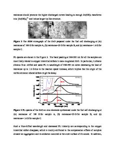
Introduction Thin films of semiconducting metal oxides are frequently used to modify the interfaces of organic semiconductor devices due to the large variety of materials with well-characterized optical and electronic properties and good chemical and physical stability.[1] Metal oxide films deposited from nanoparticle (NP) suspensions in theory combine the properties of metal oxides with large-area and low-temperature processing, which not only improves compatibility with organic devices but also create processing challenges. For example, organic photovoltaics (OPVs) represent a promising route toward low-cost, lightweight renewable energy generation.[2,3] Contact layers between bulk heterojunction (BHJ) active layers and electrodes can significantly improve performance of OPVs.[4] To fully realize the potential benefits of vacuum-free processing for lowcost OPVs, solution-processed contact layers are intensively researched in recent years.[2,3,5,6] Various solution-processed metal oxide films with high work function Φ have been utilized as hole contact layers (HCLs) in OPVs, which exhibit higher open-circuit voltage Voc,[7] higher fill factor FF,[6–12] and improved device stability[9,10] compared with the well-established conducting polymer poly(3,4-ethylenedioxythiophene):poly (styrene sulfonate) (PEDOT:PSS) HCL. Despite the recent progress, the stringent processing requirements of organic semiconductor devices have prevented general adoption of solution-processed metal oxide films as interfacial layers. For example, published reports on solutionprocessed metal oxide NP films as HCLs in OPVs typically require harsh post-deposition treatments, including annealing
Data Loading...