Germanium Layer Exfoliation by Ion-Cut Processes
- PDF / 3,086,191 Bytes
- 6 Pages / 612 x 792 pts (letter) Page_size
- 52 Downloads / 378 Views
0994-F09-05
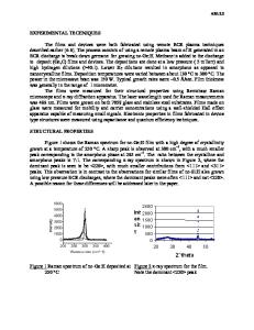
Germanium Layer Exfoliation by Ion-Cut Processes Reinhart Job, and Wolfgang D¸ngen Department of Mathematics and Computerscience, University of Hagen, Universit‰tsstr. 27, Hagen, D-58084, Germany ABSTRACT (100)-oriented Czochralski germanium (Cz Ge) wafers were implanted with hydrogen at energies up to 100 keV (related to H+) at a doses of D = 4⋅1016 H+/cm2. Post-hydrogen annealing in normal air atmosphere on a hotplate was employed for 10 min at various temperatures between 350 ∞C and 600 ∞C to investigate the samples with regard to blistering and layer exfoliation having in mind the Smart-CutTM technology for GOI structure formation. The generation and evolution of blisters and craters ("exploded" blisters demonstrating layer exfoliation) were investigated in dependence on the annealing temperature by atomic force microscopy and µ-Raman spectroscopy. The latter method points out the appearance of strong tensile stress upon H+ implantation and subsequent annealing. If the tensile stress exceeds about 1.2 GPa layer exfoliation occurs. INTRODUCTION Due to progressive scaling MOS based Si devices are reaching their physical limits. Therefore, with regard to further progress the semiconductor industry has to consider far reaching measures, for instance the alteration of the wafer material (SiGe alloys or strained Si [1]) or even the replacement of Si (by GaAs ?). For further use of large parts of the infrastructure of Si technology another option might be attractive, i.e. the application of Ge wafers, since quite large wafers are already available (∅ = 200 mm), pn-junctions can be easily created using common element (B, P, etc.) and proper metallization can be enable by germanides with familiar materials [2]. The potentially fatal disadvantage of Ge, i.e. the quite narrow bandgap and hence the increased leakage, can be managed by using Ge-on-insulator (GOI) wafer substrates; and the Smart-CutTM technology is a promising approach for the fabrication of GOI wafers [3-6]. We have prepared GOI test structures, fabricated by H+ implantation (E = 100 keV, D = 4⋅1016 H+/cm2), wafer bonding on PyrexTM glass and annealing (10 min, 600 ∞C). However, for the current investigation on Ge layer exfoliation the wafer bonding step was omitted because for our analyses we wanted to have free access to the surface layers of the treated Cz Ge samples. EXPERIMENTAL Our investigations were done with (100)-oriented n-type Czochralski (Cz) grown Ge wafers (Sb doped, 6 ñ 10 Ωcm). The Cz Ge wafers were implanted with hydrogen at energies of 15 keV, 50 keV and 100 keV (related to H+) and doses of 4⋅1016 H+/cm2. The implanted Cz Ge wafers were cut into smaller pieces (1×1 cm2) and subsequently annealed for 10 min in air on a hotplate at various temperatures between 350 ∞C and 600 ∞C. The samples were analyzed at room temperature by µ-Raman spectroscopy (µRS) using the Dilor Labram system with Ar+ ion laser excitation (488 nm, 25 mW). The setup operates under backscatter conditions and has a resolution
a) Tanneal = 400 ∞C
b) Tannea
Data Loading...