Growth and Characterization of bulk GaN by Ga Vapor Transport
- PDF / 769,761 Bytes
- 6 Pages / 612 x 792 pts (letter) Page_size
- 87 Downloads / 438 Views
E11.33.1
Growth and Characterization of bulk GaN by Ga Vapor Transport Phanikumar Konkapaka1, Huaqiang Wu1, Yuri Makarov2, Michael G. Spencer1 Dept. of Electrical and Computer Engineering, Cornell University, Ithaca NY 14853. 2 Semiconductor Technology Research, Richmond VA 1
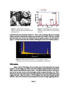
Abstract Bulk GaN crystals of dimensions 8.5 mm x 8.5 mm were grown at growth rates greater than 200µm/hr using Gallium Vapor Transport technique. GaN powder and Ammonia were used as the precursors for growing bulk GaN. Nitrogen is used as the carrier gas to transport the Ga vapor that was obtained from the decomposition of GaN powder. During the process, the source GaN powder was kept at 11550C and the seed at 11800C. Using this process, it was possible to achieve growth rates of above 200 microns/hr. The GaN layers thus obtained were characterized using X-Ray diffraction [XRD], scanning electron microscopy [SEM], and atomic force microscopy [AFM]. X-ray diffraction patterns showed that the grown GaN layers are single crystals oriented along c direction. AFM studies indicated that the dominant growth mode was dislocation mediated spiral growth. Electrical and Optical characterization were also performed on these samples. Hall mobility measurements indicated a mobility of 550 cm2/V.s and a carrier concentration of 6.67 x 10¹⁸/cm3 1. Introduction GaN is a wide bandgap semiconductor material that is used for fabrication of laser diodes [LD], light emitting diodes [LED] and high power, high frequency electronic devices [1-3]. Due to the absence of free standing GaN substrates, these devices are fabricated on foreign substrates such as SiC, Sapphire, LiGaO2 or LiGaO3 [4-7]. Performance of these devices are reduced due to high dislocation densities resulting from lattice mismatch and thermal expansion coefficient mismatch between the GaN and substrate. In order to improve the performance of devices such as LDs, LEDs and HEMTs, homoepitaxial device layers grown on high quality free standing GaN substrates are needed. Several efforts are underway to produce freestanding GaN substrates. Hydride Vapor Phase Epitaxy [8], High Nitrogen Pressure Solution Growth [9], Sublimation Technique [10] are being investigated for grow of bulk GaN crystals. Freestanding GaN crystals were also prepared by reaction of Ga vapors with ammonia [11], Ga with ammonia [12], sublimation of GaN powder [13] and growth in sodium flux [14]. Out of the above-mentioned techniques, sublimation technique gave GaN crystals with high growth rates. However, liquid Ga was a poor precursor of Ga because of its instability. Further, it was reported that pure GaN powder, when used as the precursor has led to a partial decomposition of source material into liquid Gallium and molecular nitrogen. Therefore, Baranov et al [10] have grown GaN using a mixture of GaN powder and liquid Ga. In the present work, GaN was grown by transporting Ga vapor that was obtained from decomposing GaN powder to the seed. Since bulk GaN was grown by physically transporting Ga vapor towards the seed, we call this
Data Loading...