Growth and low temperature photoluminescence of silicon nanowires for different catalysts
- PDF / 628,803 Bytes
- 6 Pages / 612 x 792 pts (letter) Page_size
- 14 Downloads / 298 Views
1178-AA04-10
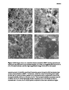
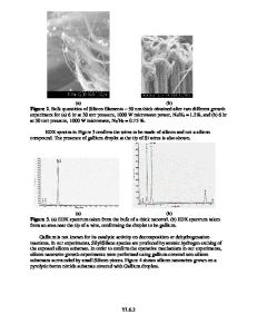
Growth and low temperature photoluminescence of silicon nanowires for different catalysts. O. Demichel a, F. Oehler a, V. Calvo a, P. Noé a, A. Besson a, N. Pauc a, P. Gentile a, T. Baronb and N. Magnea a a CEA-Grenoble, INAC/SP2M/SiNaPS, 17 rue des Martyrs, 38054 Grenoble Cedex 9, France b CNRS-LTM, 17 rue des Martyrs, 38054 Grenoble Cedex 9, France ABSTRACT We report the growth of silicon nanowires (SiNWs) by chemical vapor deposition (CVD) with several catalysts. We performed low temperature photoluminescence (PL) experiments on as-grown SiNWs for the following catalysts: Au, Cu, TiSi, PdSi and PtSi. Nanowires are chemically treated with an aqua regia solution to remove the catalyst droplets, this step is followed by a thermal oxidation process. We compared the PL of as-grown and processed SiNWs for each catalyst. INTRODUCTION Silicon nanowires (SiNWs) have attracted a large scientific interest as promising new structures for various applications such as nano-sensors or for electronics and opto-electronics devices thanks to their very interesting integration properties. As an alternative to top-down approach by etching techniques, SiNWs can be produced by Chemical Vapor Deposition (CVD) via the Vapor-Liquid-Solid (VLS) or the Vapor-Solid-Solid (VSS) mechanisms [1-4]. The catalytic materials at the basis of those two growth mechanisms can be of various sort and their influence on SiNWs properties remains to be probed. In this paper we propose a systematic study of growth and photo-luminescence (PL) properties of CVD SiNWs using the following catalysts: Au, Cu, Ti, Pt and Pd. The PL of as-grown SiNWs is compared to that from thermally oxidized nanowires. EXPERIMENT & RESULTS: Nanowire growth and oxidation: Silicon nanowires were grown in a Low Pressure Chemical Vapour Deposition (LPCVD) reactor using a H2 carrier gas flow at 20mbar. All samples are grown on Si [100] substrates. Si wafers were first deoxidized in a HF 10% solution for 1 min before catalyst deposition. Depending on the material, catalysts were evaporated as thin film by Joule heating: Au and Cu, or sputtering: Pt, Pd, Ti. For PdSi and PtSi a supplementary annealing step was performed to form PdSi and PtSi silicide before the CVD deposit. The typical deposit sequence consists in a 1) a H2 annealing step at 800°C-900°C substrate temperature at 20mbar 2) a deposit step using SiH4 and HCl, at 650°C-800°C substrate temperature, in H2 carrier flow at 20 mbar. Table 1 summarizes growth conditions for
each catalyst studied. The geometrical aspects are also reported: tapered NWs are distinguished from the non-tapered, dimensions concern the diameter dispersion for non-tapered NWs and the order of magnitude of the tapering of other NWs. Catalyst Au Cu Cu Ti PdSi PtSi
H2 Annealing 850 °C (10 min) 900 °C (5 min) 900 °C (5 min) 900 °C (5 min) 800 °C (15 min) 800 °C (15 min)
Deposit step 650 °C (50 min) 750 °C (15 min) 750 °C (30 min) 750 °C (15 min) 800 °C (15 min) 800 °C (25 min)
p(SiH4) 0.25 mbar 0.125 mbar 0.125 mbar 0.125 mbar 0.125 mbar 0.
Data Loading...