Growth defects in CuInSe 2 thin films
- PDF / 1,818,981 Bytes
- 5 Pages / 612 x 828 pts Page_size
- 11 Downloads / 450 Views
CuInSe2 thin film solar cells with an efficiency of about 10% were studied with a cross-sectional high resolution transmission electron microscope (HRTEM). The growth defects such as twins, stacking faults, and intergrowth phase in the CuInSe2 thin films were studied in detail. Polycrystalline CuInSe2 films were deposited on a Mo-coated glass substrate by using the three source evaporation system. The CuInSe2 film contains fivefold multiply twinned crystallites as well as a high density of twins in the {112} plane. The CuInSe2 film also contains intergrowth phase with a long range of periodicities of 10 A parallel to the [112] direction of the chalcopyrite structure. The intergrowth phase composition is similar to the chalcopyrite phase. The structural model of the intergrowth phase is proposed on the basis of the high resolution electron micrograph.
I. INTRODUCTION Because of its reasonable band gap (1.04 eV) and high absorption coefficient for solar radiation,1'2 the photovoltaic application of CuInSe2 thin films has been a focus of increasing interest recently. The conversion efficiency of about 15% was achieved by a CdS/CuInSe 2 heterojunction device.3 A wide variety of techniques were used to fabricate CuInSe2 thin films for photovoltaic applications. Of these deposition techniques, the three source evaporation method yielded the highest efficiency device. CuInSe2 has a tetragonal chalcopyrite structure with lattice constants of a — 5.7810 A, c = 11.6422 A, and c/a — 2.014 at room temperature.4 CuInSe2 undergoes a structural phase transition to a cubic sphalerite strui .ure above 810 °C. The chalcopyrite structure is different from the sphalerite structure by an ordered substitution of sphalerite cation by two metal cations having an equal average valence. This ordered substitution by the metal sublattice causes a doubling of unit-cell dimensions in the [001] direction with respect to the cubic sphalerite structure. Microstructures such as the grain size, twins, and the stacking faults in the CuInSe2 films play highly important roles in CuInSe2 thin film solar cells. Recently, some researchers observed the microstructures of the polycrystalline CuInSe2 films by transmission electron microscope.5"8 They identified common types of planar defects such as twins and stacking faults on the {112} chalcopyrite plane. In this paper, we report on a microstructural characterization of CuInSe2 thin film in a glass/Mo/CuInSe 2 / CdS/ZnO/ITO structure solar cells with an efficiency of about 10%. The growth defects such as twins, stacking faults, and intergrowth phases are studied in detail by cross-sectional high resolution transmission electron microscope (HRTEM) and microchemical analysis. 658
http://journals.cambridge.org
J. Mater. Res., Vol. 9, No. 3, Mar 1994
Downloaded: 27 Mar 2015
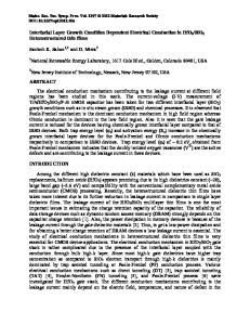
••«-,
CdS C I S
Mo...
FIG. 1. Bright-field (a) and dark-field (b) transmission electron micrographs of the cross section of CdS/CuInSe 2 /Mo layers wherein the CuInSe2 layer is indicated by the symbol CIS. © 1994 Materials Research
Data Loading...