Growth Mode and Defects in Aluminum Nitride Sublimed on (0001) 6H-SiC Substrates
- PDF / 616,031 Bytes
- 6 Pages / 792 x 792 pts Page_size
- 10 Downloads / 313 Views
Internet Journal of Nitride Semiconductor Research:
Email alerts: Click here Subscriptions: Click here Commercial reprints: Click here Terms of use : Click here
Growth Mode and Defects in Aluminum Nitride Sublimed on (0001) 6H-SiC Substrates Lianghong Liu, B. Liu, Y. Shi and J.H. Edgar MRS Internet Journal of Nitride Semiconductor Research / Volume 6 / January 2001 DOI: 10.1557/S1092578300000193, Published online: 13 June 2014
Link to this article: http://journals.cambridge.org/abstract_S1092578300000193 How to cite this article: Lianghong Liu, B. Liu, Y. Shi and J.H. Edgar (2001). Growth Mode and Defects in Aluminum Nitride Sublimed on (0001) 6H-SiC Substrates . MRS Internet Journal of Nitride Semiconductor Research, 6, pp e7 doi:10.1557/S1092578300000193 Request Permissions : Click here
Downloaded from http://journals.cambridge.org/MIJ, IP address: 137.120.4.50 on 25 Dec 2015
MRS
Internet Journal Nitride Semiconductor Research
Growth Mode and Defects in Aluminum Nitride Sublimed on (0001) 6H-SiC Substrates Lianghong Liu1, B. Liu1, Y. Shi1 and J.H. Edgar1 1Kansas
State University, Department of Chemical Engineering,
(Received Wednesday, February 21, 2001; accepted Thursday, March 29, 2001)
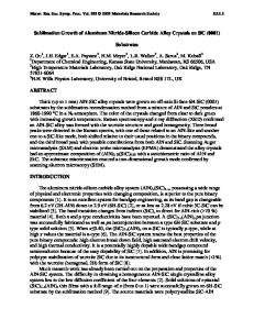
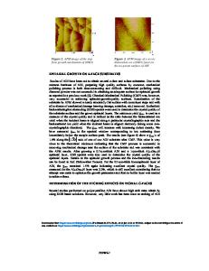
The effect of substrate preparation on the sublimation growth of AlN at about 1800 °C and 400 torr on (0001) 6H-SiC was investigated. The AlN grew in the step flow growth mode on an off-axis 6HSiC substrate with a 6H-SiC epilayer, an island growth mode on as-received substrates, and a 2-D growth mode on substrates first coated with an AlN epitaxial layer by MOCVD. Cracks in the deposited AlN crystal due to the lattice and thermal expansion coefficient mismatches were always observed by SEM and optical microscopy.
Introduction Group-III nitrides (AlN, GaN, InN, and their alloys) have attracted great interest recently for their enormous potential for optoelectronic device applications operating in the spectral range from green to ultraviolet. The lack of bulk crystals for substrates is a major limitation for fully implementing such devices; the epitaxial growth of nitrides is currently limited to foreign substrates, mainly sapphire and SiC [1]. Bulk crystal AlN will provide a superior substrate for group-III nitride epitaxial layers as it is closely lattice and thermal expansion matched to GaN. It has many favorable properties such as high thermal conductivity, low thermal expansion coefficient, high electrical resistivity, good dielectric properties, and excellent oxidation resistance. Most studies of AlN bulk crystal growth have employed the sublimation method, as AlN’s high melting temperature (>2700°C) makes it impossible to grow from melt [2] [3] [4] [5]. A bulk AlN crystal of 470 mm3 was produced by self-seeding in the sharp tip of a sealed tungsten crucible by Slack and McNelly [4] during mid-70s. The group of Schowalter and Slack et al. [6] [7] continues to improve on this technique and have reported producing crystals up to 19mm in diameter. 6H-SiC substrates offer an alternative method of seeding even larger
Data Loading...