Growth of Epitaxial Al 2 O 3 Films on Silicon by Ionized Beam Deposition
- PDF / 490,935 Bytes
- 6 Pages / 595 x 842 pts (A4) Page_size
- 74 Downloads / 403 Views
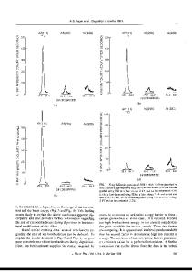
Growth of Epitaxial Al2O3 Films on Silicon by Ionized Beam Deposition SangWoo Whangbo, YunKi Choi, Kwun Bum Chung, HongKyu Jang, and ChungNam Whang Atomic-scale Surface Science Research Center and Institute of Physics and Applied Physics, Yonsei University, Seoul, 120-749, Korea ABSTRACT Epitaxial Al2O3 films have been successfully grown on an oxidized silicon substrate by the ionized beam deposition using an Al ion beam in oxygen environments. The crystalline quality dependence of the Al2O3 films on the growth temperatures was investigated. Using in situ reflection high energy electron diffraction, the orientation relationships between epitaxial Al2O3 films and Si substrate were found to be (100) Al2O3//(100) Si with [110] Al2O3//[110] Si and (111) Al2O3//(111) Si with [11 2 ] Al2O3//[11 2 ] Si. The stoichiometry of the films was found to be similar to that of sapphire from XPS measurements. INTRODUCTION High quality thin insulating layer growth on semiconductor is of great importance, with potential applications as gate dielectric materials for complementary metal oxide semiconductor (CMOS), and silicon-on-insulator (SOI) device [1-2]. For these purposes, the insulating layer needs to fit some required properties such as good crystalline quality, abrupt interface with the substrate, high dielectric constant, and surface flatness of grown films. Aluminum oxide (Al2O3) is considered to be a candidate for these applications. An attractive feature of this material is high dielectric constant and very low permeability of alkali ions, which prevents device properties from drifting and also prevents changes due to migration or diffusion of impurities. Research on epitaxial Al2O3 films on semiconductor has not been completely established. Epitaxial Al2O3 thin films for SOI device have been reported at first by M. Ishida et al., the films were grown by low-pressure chemical vapor deposition (LPCVD) [3-4]. As a source material, Al(CH3)3 (tri-methyl aluminum: TMA) and N2O gas were used. However, carbon contamination at the interface could not be avoided due to the organic by-product of its dissociation, and the epitaxial temperatures were above 1000 °C. To overcome these problems, metalorganic molecular beam epitaxy (MOMBE) [5-6] techniques using aluminum alkoxide and dimethylethylamine-alane (DMEAA) as an aluminum source and molecular beam epitaxy (MBE) [7] using Al solid source and N2O gas have been employed. In this work, Al2O3 films were grown on the oxidized Si substrate using an ionized Al P6.3.1
beam and O2 gas source. Epitaxial Al2O3 films were obtained at relatively low substrate temperatures and the high-resolution transmission electron microscopy (HRTEM) image of epitaxial Al2O3 film on Si(111) is presented. EXPERIMENTAL DETAILS The ionized beam deposition (IBD) apparatus is composed of a growth chamber and loadlock system, the growth chamber is equipped with in situ reflection high-energy electron diffraction (RHEED), and evacuated to medium 10-10 Torr. The schematic diagram of the ion source for the ionized Al
Data Loading...