Growth of NbO 2 by Molecular-Beam Epitaxy and Characterization of its Metal-Insulator Transition
- PDF / 6,165,208 Bytes
- 6 Pages / 612 x 792 pts (letter) Page_size
- 38 Downloads / 306 Views
Growth of NbO2 by Molecular-Beam Epitaxy and Characterization of its Metal-Insulator Transition Lindsey E. Noskin1, Ariel Seidner H.1, and Darrell G. Schlom1,2 1
2
Department of Materials Science and Engineering, Cornell University, Ithaca, NY 14853, U.S.A. Kavli Institute at Cornell for Nanoscale Science, Ithaca, NY 14853, U.S.A.
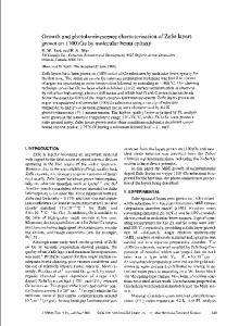
ABSTRACT Thin films of NbO2 are synthesized by oxide molecular-beam epitaxy on (001) MgF2 substrates, which are isostructural (rutile structure) with NbO2. Two growth parameters are systematically varied in order to identify appropriate growth conditions: growth temperature and the partial pressure of O2 during film growth. θ-2θ X-ray diffraction measurements identify two dominant phases in this system at background oxygen pressures in the (0.2–6)×10–7 Torr range: rutile NbO2 is favored at higher growth temperature, while Nb2O5 forms at lower growth temperature. Electrical resistivity measurements were made between 350 K and 675 K on three epitaxial NbO2 films in a nitrogen ambient. These measurements show that NbO2 films grown in higher partial pressures of molecular oxygen have larger temperature-dependent changes in electrical resistivity and higher resistivity at room temperature. INTRODUCTION Though rare, metal-to-insulator transitions (MITs) occur in some materials and can be triggered by an external stimulus, e.g., a change in temperature, pressure, or the application of light [1]. Figure 1(a) shows the temperature-dependent metal-insulator transitions of singlecrystal MIT materials gleaned from the literature [2-27]. The resistivity data shown was selected from the literature as exemplary due to its large and sudden change in resistivity. The data in Fig. 1 is limited to materials where the MIT is an intrinsic property of the material, i.e., not due to the formation of filaments, or chemical reactions, or recrystallization. For this reason, the data is restricted to high-quality single crystals, where intrinsic behavior is most likely to be exhibited. Changes in electrical resistivities due to MITs can be several orders of magnitude in size and very sharp as quantified in Fig. 1(b), where the change in the electrical resistivity and the temperature of the transition are plotted for each material. The transition region (between the start and end of the MIT, each denoted by an “x”) was calculated by finding the second derivative of a 5-point moving smooth utilizing a cubic least-squares best-fit function to the data ! " #$% &
< 1×10⁻³ , except for CaFeO3, [28, 29]. The criteria for the points marked by “x” is that !' " V8O15, BaVS3, FeS0.47Se0.53, TiS2, NbO2, V4O7 and LaCoO3, where the “x” marks for all but NbO2 were specified manually due to the broad transitions involved. For NbO2, the “x” marks were specified based on previous research using x-ray diffraction to detect the presence or absence of dimerization, which is the mechanism of the MIT of NbO2 [30]. Materials with temperature-dependent MITs have gained attention for potential use in conjunction with metal-oxide-semicond
Data Loading...