Growth of Ultra-High Density 3C-SiC Nanowires via Single Source CVD
- PDF / 2,195,994 Bytes
- 6 Pages / 612 x 792 pts (letter) Page_size
- 104 Downloads / 325 Views
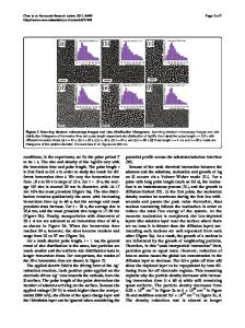
Growth of Ultra-High Density 3C-SiC Nanowires via Single Source CVD Kasif Teker1 and Joseph A. Oxenham1 1 Department of Physics and Engineering, Frostburg State University, 101 Braddock Road, Frostburg, MD 21532, U.S.A. ABSTRACT Silicon carbide (SiC) nanostructures attract interest due to their applications in optoelectronic devices, sensors, and high-power/high temperature electronics. The synthesis of SiC nanowires by chemical vapor deposition using hexamethyldisilane (HMDS) as a source material on SiO2/Si substrate has been investigated. Various catalyst materials, including iron (film and nanoparticles), nickel (film and nanoparticles), and cobalt nanoparticles have been used. The growth runs have been carried out at temperatures between 900 and 1100oC under H2 as carrier gas. 3C-SiC nanowires have successfully been grown at even lower temperatures despite the lower efficiency of source decomposition at low temperatures. The SiC nanowire diameters are in the range of 8 nm to 60 nm, as determined by transmission electron microscopy (TEM). In general, the efficiency of nanowire growth has increased with temperature except the growth on Ni film, which has occasionally resulted in SiC flowers. Higher nanowire density at high temperatures can be attributed to more efficient decomposition of the source at higher temperatures. Further, optical properties of the nanowires have been studied by Fourier transform infrared spectroscopy (FTIR). The fabricated nanowires have also been characterized by scanning electron microscopy (SEM), atomic force microscopy (AFM), and x-ray diffraction (XRD). INTRODUCTION Silicon carbide is a well-known wide band-gap semiconductor material with many superior properties, such as high electron mobility, high thermal conductivity, high mechanical strength, and high radiation resistance [1-4]. These superior properties make SiC an excellent material for applications in many areas including optoelectronics, thermoelectric devices, and microelectronics (high temperature, high power, and high frequency). Furthermore, nanoscale materials exhibit excellent physical properties. Thus, SiC nanowires present some advantages for applications such as gas sensors, blue LEDs, UV photodetectors, and field emission devices [5-7]. Synthesis of SiC nanostructures with various fabrication methods has been reported. These fabrication methods include chemical vapor deposition [8-9], carbon thermal reduction [10], metalorganic chemical vapor deposition (MOCVD) [11]. CVD has been the most widely used method to fabricate nanostructured materials due to its low cost, high yield, and simplicity of operation. Moreover, the CVD process enables direct device fabrication on pre- patterned substrates. This paper presents CVD growth of SiC nanowires using hexamethyldisilane as source material with various catalyst materials. We have studied the effects of various catalyst materials and growth temperatures on SiC nanowire growth. Furthermore, the
study also investigates the lower limit decomposition temperature of the HMDS
Data Loading...