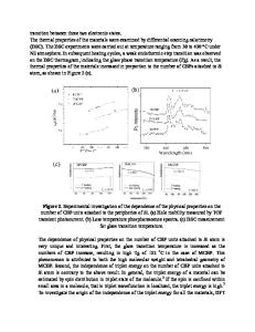
High Efficiency Blue Organic Light Emitting Devices doped by BCzVBi in Hole and Electron Transport Layer
- PDF / 6,770,768 Bytes
- 6 Pages / 612 x 792 pts (letter) Page_size
- 95 Downloads / 443 Views
High Efficiency Blue Organic Light Emitting Devices doped by BCzVBi in Hole and Electron Transport Layer Nam Ho Kim1, You-Hyun Kim1, Ju-An Yoon1, Sang Youn Lee1, Hyeong Hwa Yu2, Ayse Turak2 and Woo Young Kim1, 2* 1
Department of Green Energy & Semiconductor Engineering, Hoseo University, Asan, Korea 2 Department of Engineering Physics, McMaster University, Hamilton, Canada
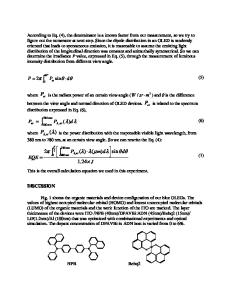
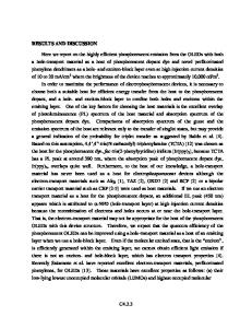
ABSTRACT The electroluminescent characteristics of blue organic light-emitting diodes(BOLEDs) were fabricated with single emitting layer using host-dopant system and doped charge carrier transport layers. The structure of the high efficiency BOLED device was; NPB(600 Å )/NPB:BCzVBi7%(100 Å )/ADN:BCzVBi-7%(300 Å )/BAlq:BCzVBi-7%(100 Å )/BAlq(200 Å )/Liq(20 Å )/Al(1200Å) to optimize probability of exciton generation by doping BCzVBi in emitting layer and hole/electron transport layers(HTL/ETL) as well. Luminance and luminous efficiency of BOLED doped BCzVBi in EML and HTL/ETL improved from 10090 cd/m2 at 9.5V and 6.44 cd/A at 4.0V to 13190 cd/m2 at 9.5V and 7.64 cd/A at 4.0V about 30% and 18%, respectively, with CIE coordinates of (0.14, 0.17) comparing to BOLED doped BCzVBi in EML only INTRODUCTION Organic light-emitting diodes (OLEDs) attract a high level of research enthusiasm due to their thin-film effects, high-contrast, light-weight, fast-response time, wide-viewing-angle and lowvoltage attributes. [1-4] They have been regarded as one of the most promising flat panel display technologies that are capable of meeting the demands of future display applications. [5-6] Especially, there has been much effort to improve the internal and external quantum efficiency of blue organic light-emitting diodes (BOLEDs) by changing various emitting materials and adapting new device structures improving out-coupling efficiency. Also, selection of dopant materials used for charge transport layers has been restricted because they should have high charge mobility and a proper energy band. [7-9] In this study, we fabricated wide recombination zone (WRZ) BOLEDs by doping BCzVBi into not only emitting layer but hole and electron transport layer. Generally, hole-electron recombination are confined in only EML due to hole and electron blocking by charge transport layers whose thicknesses are optimized for exclusive emission in EML and higher HOMO-LUMO energy gap of transport layers than that of emissive dopant. [10-11] However, recombination zone was extended to HTL and ETL by doping BCzVBi into these layers and it affected charge balance in organic layers of BOLEDs EXPERIMENT Indium Tin Oxide (ITO) coated glass was cleaned in an ultrasonic bath by the regular cleaning sequence: in deionized water, isopropyl alcohol, acetone, deionize water, isopropyl alcohol, thereafter, the pre-cleaned ITO was treated with an O2 plasma, under vacuum conditions of 5.0 × 10⁻² Torr, of 50W for 2 minutes. BOLED devices were fabricated by thermal evaporation under high vacuum conditions of 5.0 × 10⁻⁷ Torr. BOLEDs were composed of N, N’-diphenyl -N,N’-
bis(l-naphthyl-phenyl)-(l,l’-biph
Data Loading...