High Efficiency Sputtered CdS/CdTe Cells without CdCl 2 Activation
- PDF / 304,091 Bytes
- 6 Pages / 432 x 648 pts Page_size
- 26 Downloads / 337 Views
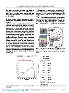
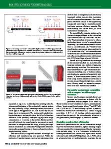
High Efficiency Sputtered CdS/CdTe Cells without CdCl2 Activation N.R. Paudel, K.A. Wieland & A.D. Compaan Department of Physics and Astronomy, University of Toledo, Toledo, OH 43606 USA ABSTRACT Polycrystalline thin-film CdS/CdTe PV cells nearly always require “activation” with vapors containing chlorine and oxygen near 400 oC in order to realize the highest cell performance, even when growth occurs near 600 oC. In this study we have used film growth near 270 oC by magnetron sputtering in an oxygen-free ambient and have studied the effects of post-deposition heat treatments for 20 minutes at 400, 425 and 450 oC without CdCl2 in a dry air ambient. The heat treatments enhanced grain growth and produced re-crystallization of the CdTe film at all three temperatures, but 450 oC was required to reach the best electrical performance. Grain size increased from a couple of hundred nanometers to more than a micron as the preferred (111) growth orientation decreased. Efficiencies up to 11.6% were achieved with no CdCl2 compared to ~13% with activation at 387 oC in the presence of CdCl2 vapors. X-ray diffraction and quantum efficiency measurements show interdiffusion of CdS and CdTe at 450 oC comparable with a standard CdCl2 treatment at 387 oC. The results are discussed in terms of CdSTe alloy gradients and minority-carrier diffusion lengths. INTRODUCTION Among the polycrystalline thin-film semiconductors CdTe has a nearly ideal band gap and easily passivated grain boundaries. Furthermore the growth technology is inexpensive and flexible with many deposition methods yielding good results over a wide range of growth temperatures. Among them, magnetron sputtering is a relatively low-temperature deposition method with excellent control of growth rate, grain size, and film stress [1]. However, with any growth method, CdTe films typically need to be “activated” with a high temperature CdCl2 treatment in order to obtain the best efficiencies [2]. With this activation, CdS/CdTe cells have been fabricated, e.g., with 16.5% efficiency by close-spaced sublimation [3] and 14% efficiency by sputtering [4]. The CdCl2 vapors and oxygen promote grain boundary passivation and may also lead to recrystallization of the CdTe film [5]. CdCl2 activation also promotes interdiffusion of S and Te which decreases the lattice mismatch by reducing in-plane compressive stress of CdTe film [6, 7]. Chloride activation significantly enhances the minority carrier lifetime in CdTe and reduces the grain-boundary recombination [8]. Although the activation process is almost universally used in device fabrication, the basic understanding of the role of regrowth and of oxygen and chlorine is poorly understood. Here we approach the issue by starting with small grain material grown at relatively low temperature and compare film and device characteristics after annealing or activating with and without CdCl2. EXPERIMENTAL DETAILS The CdS/CdTe films were sputtered on Pilkington TEC12 soda-lime glass substrates coated with a 50 nm highly resistive buffer layer at 270 o
Data Loading...