High Power 325 Light Emitting Diode Arrays by Flip-Chip Packaging
- PDF / 61,128 Bytes
- 5 Pages / 612 x 792 pts (letter) Page_size
- 84 Downloads / 270 Views
L7.7.1
High Power 325 Light Emitting Diode Arrays by Flip-Chip Packaging Ashay Chitnis, Maxim Shatalov, Vinod Adivarahan, Jian Ping Zhang, Shuai Wu, Jie Sun, and M. Asif Khan Department of Electrical Engineering, University of South Carolina, Columbia, SC 29208, U.S.A. ABSTRACT We report flip-chip 325 nm emission light emitting diodes over sapphire with dc powers as high as 0.84 mW at 180mA and pulse powers as high as 6.68 mW at 1A. These values to date are the highest reported powers for such short wavelength emitters. Our data shows the device output power under dc operation to be limited by the package heat dissipation. A study is presented to determine the role of thermal management in controlling the power output for the reported 325 nm ultraviolet light emitting diodes.
INTRODUCTION Recently, there have been a number of reports of deep ultraviolet (UV) (280 nm < λ < 350 nm) III-N quantum well light-emitting diodes (LEDs) on sapphire, SiC and bulk GaN substrates [1-9]. In these substrate choices, SiC and HVPE GaN have superior thermal conductivity and they also allow for vertical conduction device geometry. However, both of these substrate types are highly absorbing in the deep ultraviolet wavelength region and thus require the output power extraction through the top p-contact and the p+-GaN contact layer. In contrast, we have shown sapphire to be a good substrate choice for deep UV LEDs with efficient light extraction through the substrate [5,6,8-10]. However, under dc operation, sapphire substrate based deep UV LEDs suffer from excessive self-heating due to its lower thermal conductivity and relatively high operating voltages. Recently, using micro-Raman spectroscopy and electroluminescence (EL), we have reported that the self-heating in 325 nm emission UV LEDs can increase the device temperature by about 70°C for a dc bias current of 50 mA [10]. We now report a significant improvement in the performance of the sapphire substrate based 325 nm LEDs by the use of a low thermal resistance package. A customized silver (Ag) plated copper header and flip-chip packaging enabled us to obtain record dc and pulsed powers of 0.84 mW and 6.68 mW for room temperature operation.
EXPERIMENTAL DETAILS The epilayer structure for the LEDs of our study was grown over basal plane sapphire substrates using the low-pressure metal organic chemical vapor deposition technique. Similar to our previous report a 10 period AlN (20 Å)/Al0.2Ga0.8N (300 Å) superlattice (SL) and a 2 µm thick n+-Al0.2Ga0.8N over layer were used to reduce the threading dislocation density by a factor of five [11]. The device active layers consisted of three Al0.18Ga0.82N (110 Å)/ Al0.12Ga0.88N (35 Å) quantum wells. These were capped with a 200 Å thick Mg-doped p-Al0.3Ga0.7N and a 500 Å thick p+-GaN layer. Square geometry mesa devices with edge dimensions ranging from
L7.7.2
100 µm to 300 µm were then fabricated. The mesa etching, contact metalization and annealing procedures were identical to those reported earlier [5-7].
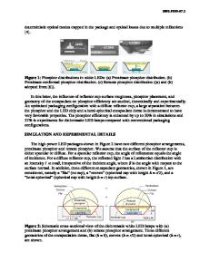
DISCUSSION The fabricated wafer
Data Loading...