High-resolution Raman imaging by optically tweezing a dielectric microsphere
- PDF / 396,964 Bytes
- 5 Pages / 612 x 792 pts (letter) Page_size
- 49 Downloads / 307 Views
1025-B11-02
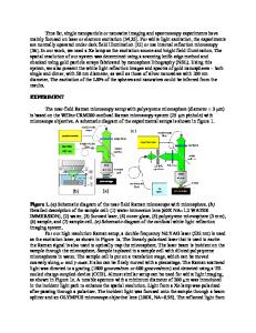
High-resolution Raman imaging by optically tweezing a dielectric microsphere J. Kasim1,2, T. Yu1, Y. M. You1, J. P. Liu2, A. K. H. See2, and Z. X. Shen1 1 Physics and Applied Physics, Nanyang Technological University, 1 Nanyang Walk, Blk 5 Level 3, Singapore, 637616, Singapore 2 Chartered Semiconductor Manufacturing Ltd., 60 Woodlands Industrial Park D, Street 2, Singapore, 738406, Singapore ABSTRACT We demonstrate a different method to perform near-field Raman imaging with subdiffraction limit spatial resolution. In this method, a dielectric microsphere (for example polystyrene microsphere) is trapped by optical tweezers. The microsphere is used to focus the laser to the sample, and also to collect the scattered Raman signals. We show the capability of this method in imaging various types of samples, such as SiGe/Si structures, gold nanopattern and carbon nanotubes. This method is comparatively easier to perform, has better repeatability, and generates stronger signal as compared to the normal near-field Raman techniques. INTRODUCTION Raman microscopy has been used extensively for material characterization in research and industry. It provides information on some critically important material specific properties such as composition, chemical bonding, electronic and atomic structures and strain/stress. This information cannot be obtained/or easily obtainable by other conventional microscopic techniques such as atomic force microscopy (AFM), scanning electron microscopy (SEM), transmission electron microscopy (TEM), and confocal optical microscopy. Raman microscopy is also a technique that is non-destructive and sample preparation free, unlike some of the techniques listed above which require extensive sample preparation and are destructive. Hence Raman microscopy is a very useful technique, complementary to the existing techniques. The main stumbling block of employing Raman microscopy in the nanoscience and nanotechnology is the spatial resolution, which is limited by the diffraction of light at ~λ/2, where λ is the wavelength of the laser light being used, which is typically about 500 nm. Several techniques have been employed to improve the spatial resolution by utilizing the nearfield techniques. Among them, laser delivered through metal-coated tapered optical fiber (aperture) [1-3] and tip-enhanced (apertureless) [4-6] near-field Raman techniques are the most frequently used. The main problem associated with the (aperture) optical fiber technique is that the laser intensity obtainable is extremely weak, resulting in very poor S/N ratio in the Raman spectrum. As a result it requires extremely long imaging time. The tip enhancement using the apertureless approach has low success rate due to several reasons: (1) the difficulty in controlling the geometry of the metal tip apex that is in nanometer scale, (2) the signal is not purely nearfield (signal that carries the high spatial resolution). It also contains far-field signal that carries low spatial resolution and should be reduced as much as possible.
Data Loading...