High Sensitivity Convergent Beam Electron Diffraction for the Determination of the Tetragonal Distortion of Epitaxial Fi
- PDF / 1,646,097 Bytes
- 6 Pages / 417.6 x 639 pts Page_size
- 70 Downloads / 327 Views
monocrystalline- lattice [1]. This excess As tends to expand the epitaxial LT-GaAs lattice. Thus the pseudomorphic LT-GaAs layer experiences a tetragonal strain, i.e. an elongation of the lattice along the growth direction (c-axis). The degree of tetragonal distortion, Ac/c, is directly correlated with the excess As content ([As]/([Ga])-I of the layer [2]. This tetragonal distortion is quite small, in our case 0.04%, as will be shown in the following, and is usually determined by high-resolution x-ray diffraction (HR-XRD) [3]. However, this method has the drawback to average over the entire thickness of the epitaxial layer and to sample a rather large area. As we are interested in a possible change of the As content along the growth direction, we apply convergent beam electron diffraction (CBED) to determine the tetragonal distortion with high spatial resolution, typically 10nm. In an earlier paper [4] the capability of CBED to resolve the tetragonal distortion of LTGaAs layers has already been demonstrated. But as it was found in the same work [4] a kinematic approach is not sufficient to achieve consistent quantitative results. In the present work, we determine the tetragonal distortion by quantitatively comparing the experimental CBED patterns with computer simulations based on dynamical diffraction. In order to determine the positions of the defect lines to be evaluated we use Hough transformations of both experimental and simulated patterns, following a suggestion of Krimer and Mayer [5]. The simulations were performed using the ems program package of P.A.Stadelmann [6]. 93 Mat. Res. Soc. Symp. Proc. Vol. 589 © 2001 Materials Research Society
EXPERIMENTAL
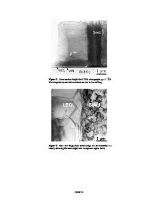
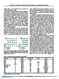
We shall discuss results obtained from an LT-GaAs layer grown at a nominal substrate temperature of 180°C onto a semi-insulating GaAs substrate. For CBED experiments, we prepared transmission electron microscopy (TEM) cross-sections of the LT-GaAs layer structure (see Fig. 1). Such a section perpendicular to the growth surface displays the vertical structure of the sample. The substrate, AlAs' and LT-GaAs layers are sketched in Fig. 1. The filled circles symbolize the depth distribution of potential positions for diffraction patterns. In contrast to conventional transmission electron diffraction (TED) with an almost parallel beam, for CBED the electron beam is focused onto the specimen. Thus the diffraction spots expand into diffraction discs. These discs show a structure of dark (defect) and bright (excess) higher order Laue zone (HOLZ) lines. The positions of these lines are very sensitive to changes of the lattice parameters. In the following, we will focus on the HOLZ line pattern of the central (000) diffraction disc, which shows defect lines only (Fig. 2). For our purpose the projection of the [120] zone is favorable [4].
1-
{ 1 mLT-GaAs
C)
70nm AlAs
[110]
substrate s.i. GaAs
Figure 1 Schematic layer structure of the LT-GaAs sample. The filled circles mark potential positions for diffraction patterns.
Figure 2 Experimental CBED pattern of the
Data Loading...