Polarity Determination for MOCVD Growth of GaN on Si(111) by Convergent Beam Electron Diffraction
- PDF / 1,713,723 Bytes
- 6 Pages / 612 x 792 pts (letter) Page_size
- 55 Downloads / 342 Views
F99W3.3
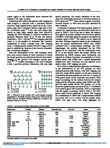
Figure 1. projection of the GaN structure. [0001] is defined as the direction of Ga to N bond between Ga/N bilayers, as shown with the arrow in the figure. was ~60 nm. The AlN layer was crack-free over the entire wafer, and the RMS roughness measured by AFM was on the order of 15 nm. The wafers were then coated with 200 nm-thick SiO2 using plasma-enhanced chemical vapor deposition, and 5 µmwide stripes oriented in the Si direction were patterned using standard UV photolithography and wet chemical etching. The width of the SiO2 mask regions was 35 µ m. The LEO GaN stripes were obtained by performing a regrowth at ~1060°C using TMGa and NH3. TEM samples were prepared by wedge polishing followed by Ar+ ion milling. Diffraction contrast images and CBED patterns were obtained on a JEOL 2000FX microscope operated at 200 kV. The surface topography was imaged using a Digital Instruments Dimension 3000 AFM operating in tapping mode. Simulations were done by software package “Desktop Microscopist 2.0” [9]. The simulated CBED patterns were calculated by solution of the many-beam equation with 33 zero-order reflections. It is well known that the polarity of GaN/Al2O3 grown by MOCVD is usually Ga face. We also checked the polarity of our MOCVD grown GaN on Al2O3 by CBED and confirmed that it is Ga face. RESULTS AND DISCUSSION Cross-section TEM micrographs are shown in Figure 2. The seed region has a threading dislocation density on the order of ~1011 cm-2, consisting predominantly of pure edge dislocations. In contrast, the LEO regions have a very low threading dislocation
F99W3.3
Figure 2. Cross-section bright-field TEM micrographs, g = 11 2 0. The irregular top and side surfaces are due to ion milling.
Figure 3. Plan-view bright field TEM image of LEO GaN/Si(111) clearly showing the seed (right) and overgrown region (left).
F99W3.3
Figure 4. Experimental and simulated CBED patterns at different thickness. All patterns correspond to [1 1 00] zone axis.
F99W3.3
density and show an essentially single-crystalline microstructure. The plan-view TEM image (Figure 3) further confirmed that the threading dislocation density was reduced several orders of magnitude in the LEO region. No inversion domain boundaries were observed under both cross-section and plan-view TEM. We reasonably assume that the GaN/Si(111) grown by MOCVD has one unique polarity. Figure 4 shows the comparison of experimental and simulated CBED patterns. The experimental CBED patterns were taken under zone-axis at 200 kV from different thickness region of the cross section sample. One should pay attention when indexing the diffraction pattern. For some models of transmission electron microscopes, there is a 180° inversion between image and diffraction pattern. This can be checked by underfocusing the diffraction lens to image a plane above the diffraction pattern. The image will not be inverted with respect to the diffraction pattern [10]. The simulations were calculated with 33 zero-order reflections and mean absorption coefficient 0.05. A series
Data Loading...


