High Spatial Resolution Mapping of Porous Silicon
- PDF / 2,922,394 Bytes
- 6 Pages / 420.48 x 639 pts Page_size
- 93 Downloads / 430 Views
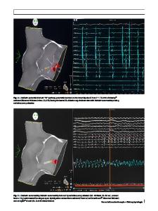
HIGH SPATIAL RESOLUTION MAPPING OF POROUS SILICON E. ETTEDGUI*, C. PENG**, L. TSYBESKOV*, Y. GAO* and P.M. FAUCHET** University of Rochester, Rochester, NY 14627 *Department of Physics and Astronomy "**Department of Electrical Engineering G.E. CARVER AT&T Bell Laboratories, Princeton, NJ 08540 H.A. MIZES Xerox Webster Research Center, Webster, NY 14580 ABSTRACT Porous silicon (PSI) samples with high photoluminescence (PL) efficiency were examined using microscopic mapping techniques including scanning electron microscopy (SEM) and spatially resolved photoluminescence (SRPL). Studies of the growth conditions indicate that the homogeneity of the PL and the surface roughness of the sample depend on the preparation procedure of the PSI layer. SEM and spatially-resolved reflectance scans of an n-type sample with a PSI layer on the order of 100 gm reveal a highly fractured surface. SRPL of the same sample shows non uniform PL on a scale of 5 gim. Cross-sectional analysis of the samples with SRPL and SEM reveals the intricate multilayer structure of the PSI film. The top portion of the PSI film is largely responsible for the PL and is composed of isolated column-like structures. We have also observed cross-shaped structures reminiscent of stress fractures on the surface of PSI films using SEM or optical microscopy. Furthermore, atomic force microscopy (AFM) and SEM measurements of the surface of PSI films of intermediate thickness reveal that samples which appear smooth on - Igm scale are actually covered with clumped structures on the order of 100 to 150 nm. INTRODUCTION The preparation techniques of light-emitting PSI have progressed greatly since PL was initially reported in 1990 [1]. Although highly efficient PL is now routine, progress in the implementation of devices made from PSI has been hampered [2,3], in part because modern electronic devices require high quality interfaces. The surface roughness resulting from the preparation of PSI samples has created one of the major obstacles in the widespread application of this new technology, for example by making good contacts nearly impossible to manufacture. High spatial resolution mapping of the PSI layers can help us characterize the surface microstructure and thus determine the optimum conditions for obtaining smooth surfaces. In addition, it is not clear which regions of the PSI layer produce light. Since the PSI layer contains a variety of microstructures, high spatial resolution mapping has the potential of identifying the light-emitting structures and eventually the preparation conditions that lead to a high density of them. A possible benefit would be full characterization of the light-emitting structures and thus a direct answer to the question of the origin of the PL [4,5]. For the investigation of surfaces, a variety of direct and indirect probes are available. Direct surface observation is most easily accomplished with optical microscopy. Alternatively, an electron beam can replace the light; the advantage of scanning electron microscopy (SEM) is its higher
Data Loading...