High spatial resolution ultrafast scanning tunneling microscopy
- PDF / 435,275 Bytes
- 12 Pages / 612 x 792 pts (letter) Page_size
- 11 Downloads / 431 Views
G3.1.1
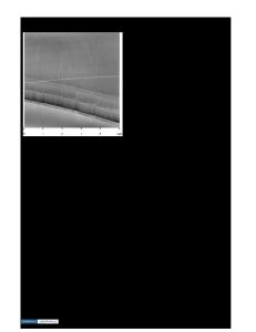
High spatial resolution ultrafast scanning tunneling microscopy Dzmitry Yarotski, and Antoinette J. Taylor* Materials Science and Technology Division, Los Alamos National Laboratory, Los Alamos, NM ABSTRACT We demonstrate ultrafast dynamical imaging of surfaces using a scanning tunneling microscope with a low-temperature-grown GaAs tip photoexcited by 100-fs, 800-nm pulses. We detect picosecond transients on a coplanar stripline and demonstrate a temporal resolution (full-width at half maximum) of 1.7 ps. By dynamically imaging the stripline, we demonstrate that the local conductivity in the sample is reflected in the transient correlated current and that 20-nm spatial resolution is achievable for a 2 ps transient, correlated signal. We apply this technique of photoconductively-gated ultrafast scanning tunneling microscopy to study carrier dynamics in InAs/GaAs self-assembled quantum dot samples at T=300 K. The initial carrier relaxation proceeds via Auger carrier capture from the InAs wetting layer (WL) on a timescale of 1-2 ps, followed by recombination of carriers on a 900 ps timescale. Finally, we demonstrate junction-mixing ultrafast STM (JM-USTM) using picosecond voltage pulses propagating on a patterned metal-on-metal (Ti/Pt). Using JM-USTM we have achieved a spatio/temporal resolution of 1 nm/8 ps. INTRODUCTION Controlling functionality in advanced materials is essential to address the need for new materials in the next millenium. Key to controlling material functionality is the understanding of structure-function relationships in complex materials on atomic length and time scales. Since many next-generation materials involve inhomogeneity and complexity of structure, understanding structure-function relationships on these short length and time scales is a prerequisite to predicting and manipulating functionality. The invention of the scanning tunneling microscope (STM) revolutionized the field of surface science, enabling the first images of surface structure on an atomic length scale. However, investigations using STM techniques have been largely restricted to the study of static surface properties such as electronic structure and topography, revealing little information on the dynamics underlying the phenomena under study. On the other hand, ultrafast optical techniques routinely reveal material dynamics on timescales as short as 10 fs, but with a spatial resolution > 1 µm. In this paper we describe our ongoing efforts to combine ultrafast optical techniques with scanning tunneling microscopy to characterize ultrafast dynamical events occurring on atomic length scales. We describe here results based on both photoconductive gating ultrafast STM (PG-USTM) and junction mixing ultrafast STM (JM-USTM). PHOTOCONDUCTIVELY-GATED ULTRAFAST SCANNING TUNNELING MICROSCOPY In the quest for both atomic spatial and temporal resolution several groups1-6 have integrated an ultrafast optoelectronic switch in series with a metal STM tip to gate the tunneling current with picosecond time resolution, a technique calle
Data Loading...