Higher efficiency of n-i-p solar cells by Hot-Wire CVD at moderate temperatures
- PDF / 120,027 Bytes
- 6 Pages / 612 x 792 pts (letter) Page_size
- 44 Downloads / 372 Views
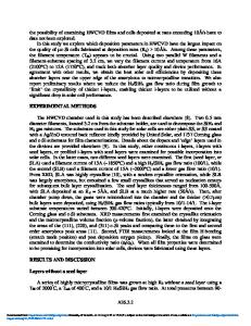
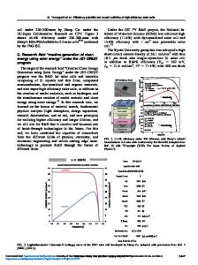
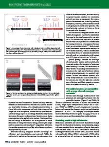
Higher efficiency of n-i-p solar cells by Hot-Wire CVD at moderate temperatures Marieke K. van Veen and Ruud E.I. Schropp Utrecht University, Debye Institute, Physics of Devices, P.O. Box 80.000, 3508 TA Utrecht, The Netherlands. ABSTRACT Hot-Wire deposited amorphous silicon is an excellent material for the incorporation as the absorbing layer in n-i-p solar cells. We decreased the deposition temperature from 430 ◦ C to 250 ◦ C, keeping device quality (opto-)electrical properties of the a-Si:H layers. This enables application of Hot-Wire deposited a-Si:H in p-i-n structures and tandem solar cells. Layers deposited at 250 ◦ C have been applied in efficient n-i-p and n-i-p/n-i-p solar cells. The deposition ˚ No optical enhancements, like texturing or back rate of the intrinsic layer was about 10 A/s. reflectors, were used. Single-junction cells with a fill factor of 0.72 and an open-circuit voltage of 0.89 V have been produced. On a flexible stainless steel substrate, an initial efficiency of 7.2 % was recorded. Tandem cells also show a high fill factor (0.71) and open-circuit voltage (1.70 V), resulting in an initial efficiency of 8.5 %. INTRODUCTION Hydrogenated amorphous silicon (a-Si:H) has proven to be a good quality and economically feasible material for the incorporation in solar cells. Although the Plasma Enhanced Chemical Vapor Deposition (PECVD) technique is commonly used for the deposition of the material, the applicability of this method for commercial use is limited due to the inherently low deposition rate. Therefore, other deposition techniques are needed to overcome this problem while maintaining the device quality of the material. The Hot-Wire Chemical Vapor Deposition (HWCVD) method, also known as catalytic chemical vapor deposition, has turned out to be a promising candidate with deposition rates of more than one order of magnitude larger than those obtained with PECVD. With this technique, however, device quality material has mainly been made at high deposition temperatures (> 350 ◦ C) [1, 2]. Since p-doped layers deteriorate at these temperatures, this technique has mainly been used for the deposition of n-i-p cells [3, 4]. Lowering of the deposition temperature is required for the application of the Hot-Wire technique in p-i-n structures and tandem solar cells. The University of Kaiserslautern has already reported high initial efficiencies for p-i-n structures [5]. At Utrecht University, incorporation of a-Si:H deposited at 430 ◦ C in an n-i-p cell yielded an initial effiency of 5.5 %, using a special thermally resistant n-layer and applying rehydrogenation treatments after i-layer deposition [6]. In this study, we investigated the effects of a lower deposition temperature in the HWCVD process on the opto-electronic properties of the hydrogenated amorphous silicon. The application of this moderate-temperature material in both single junction and tandem solar cells is examined. EXPERIMENT All silicon films used in this study were deposited in the PASTA system [7], a multichamber high vacuum deposi
Data Loading...