Highly Textured Microcrystalline Si-Thin Film Fabricated by Layer-by-Layer Technique
- PDF / 434,758 Bytes
- 6 Pages / 420.48 x 639 pts Page_size
- 91 Downloads / 383 Views
HIGHLY TEXTURED MICROCRYSTALLINE SI-THIN FILM FABRICATED BY LAYER-BY-LAYER TECHNIQUE
Shun-ichi ISHIHARA, Deyan HE, Tetsuya AKASAKA, Yuzoh ARAKI, Masami NAKATA, and Isamu SHIMIZU, The Graduate School at Nagatsuta, Tokyo Institute of Technology, 4259 Nagatsuta, Midoriku, Yokohama-city Japan 227 ABSTRACT
Microcrystalline silicon with high crystallinity was fabricated on a glass substrate at a rather low temperature (320 C) by alternately repeating the deposition of Si thin layer 10 nm thick from fluorinated precursors and the treatment with atomic hydrogen. Hydrogen content was reduced to 0.5 at% or less. According to the in situ ellipsometric observation, the sticking of precursors followed the reactions for the construction of the ordered structure with the aid of atomic hydrogen. In addition, the defects were passivated efficiently with the treatment down to 4x10 16 spins/cm 3. A marked improvement was simultaneously verified inthe efficiency of the substitutional P-doping inthe films fabricated by this layer-by-layer technique. INTRODUCTION
A novel technological field termed "Giant Micro-Electronics" has developed since the advent of hydrogenated amorphous silicon (a-Si:H), where solar cells, TFT arrays for the liquid crystal displays and image sensors attracted some attention as the promising targets.[1] However, the small carrier-mobility of a-Si:H has set a limit to the performances of these devices, and the appearance of new materials leading to the improvement of the performance is strongly expected. The poly-crystalline silicon grown on a glass substrate at a rather low temperature, 600 C, has been investigated extensively.[2],[3] The poly-Si fabricated on the glass substrate by the laser annealing, inparticular, has attracted a considerable attention due to its carriermobility as high as 300 cm2Nsec or over. Ithas not yet been to practical use for devices, however, since there are technological problems infabricating large area films with high uniformity.[4],[5] On the other hand, microcrystalline silicon (pc-Si) has some attractive characteristics, rather high mobility together with high uniformity. We can easily fabricate the /c-Si by the RF glow discharge of SiH 4 diluted with H2 in the similar manner to the fabrication of aSi:H.[6],[7]j,[8] However, its rather poor electric properties and the slow growth rate as low as 1A/sec as well set a limit to utility of this material. A marked improvement has been made inthe crystallinity of the pc-Si by adopting the remote-type plasma to avoid the ionbombardment, but on the contrary, the growth rate was markedly reduced.[9] pc-Si thin films are fabricated from the fluorinated precursors, SiHnFm (n+m
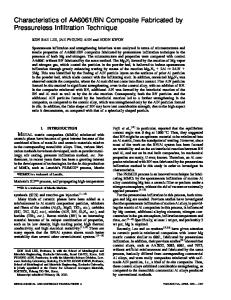
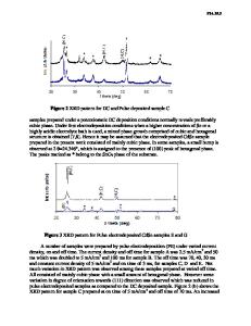
Data Loading...