Imaging And Spectroscopy Of Nanostructures Through Aberration-Corrected Stem
- PDF / 4,905,198 Bytes
- 10 Pages / 612 x 792 pts (letter) Page_size
- 90 Downloads / 308 Views
S3.1.1
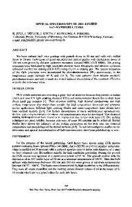
IMAGING AND SPECTROSCOPY OF NANOSTRUCTURES THROUGH ABERRATION-CORRECTED STEM S. J. PENNYCOOK1,2, M. F. CHISHOLM,1 A. R. LUPINI1, A. BORISEVICH,1 K. SOHLBERG3, J. R. MCBRIDE4, S. J. ROSENTHAL4, D. KUMAR5, A. FRANCESCHETTI2,1*, S. RASHKEEV1,2, S. WANG1,2 and S. T. PANTELIDES1,2 1 Condensed Matter Sciences Division, Oak Ridge National Laboratory, Oak Ridge, TN 2 Department of Physics and Astronomy, Vanderbilt University, Nashville, TN 3 Department of Chemistry, Drexel University, Philadelphia, PA 4 Department of Chemistry, Vanderbilt University, Nashville, TN 5 North Carolina A&T State University, Greensboro, NC * Now at National Renewable Energy Laboratory, Boulder, CO INTRODUCTION The successful development of aberration correctors for the scanning transmission electron microscope (STEM) has more than doubled the achievable spatial resolution in the last few years. Recently, the direct imaging of a crystal lattice at sub-Angstrom resolution has been demonstrated, as shown in Fig. 1.1 The sub-Angstrom probe has the same current as the uncorrected probe, but it is concentrated into a much smaller diameter. It therefore not only gives higher resolution, but also gives improved signal to noise ratio than before, sufficient to allow Z-contrast imaging of individual atoms on materials surfaces and within the bulk. It also facilitates electron energy loss spectroscopy with Figure 1. Z-contrast image of improved sensitivity, allowing single atom identification Si〈112〉 resolving the 0.78 Å dumbbell separation. with atomic spatial resolution.2 These capabilities makes the aberration-corrected STEM an ideal instrument for imaging materials and nanostructures. An unanticipated advantage of aberration correction is the much improved depth resolution, which is now at the nanometer level. Here we present several examples of the capabilities realized by such instruments, taken from different materials fields. Most of the results presented are obtained with the VG Microscopes HB603U STEM at Oak Ridge National Laboratory (ORNL), equipped with a Nion aberration corrector. This machine operates at an accelerating voltage of 300 kV and produces a beam size of 0.6 Angstroms.1 In several cases, the same system was studied theoretically using first-principles density functional calculations. The experimental and theoretical results were combined to produce significant new understanding of the underlying physical structures and phenomena. APPLICATIONS IN NANOCATALYSIS Pt trimers on γ-Al2O3. Several years ago, before installation of the aberration corrector, the HB603U STEM obtained the first images to show that Pt clusters could form trimer-like structures on the surface of a high surface area γ-Al2O3.3 That work showed that extremely small clusters, even single atoms, might be catalytically important, but the precision of the experimental data on the interatomic distances was insufficient to choose among the competing
S3.1.2
mechanisms of trimer formation. The improved sensitivity after aberration correction is striking, as shown
Data Loading...