Impact of Hydrogen Plasma Treatment on Gettering by He Implantation-Induced Cavities in Silicon
- PDF / 1,098,791 Bytes
- 6 Pages / 612 x 792 pts (letter) Page_size
- 52 Downloads / 361 Views
H4.2.1
Impact of Hydrogen Plasma Treatment on Gettering by He Implantation-Induced Cavities in Silicon D. Alquier1, E. Ntsoenzok2, C.L. Liu1,2, A. Vengurlekar3 and S. Ashok3 1
LMP, 16 rue Pierre et Marie Curie, BP 7155, F37071 Tours CEDEX, France CERI-CNRS, 3A rue de la Férollerie, 45071 Orléans CEDEX, France 3 Department of Engineering Science and Mechanics, the Pennsylvania State University, 212 Earth and Engineering Science Building, University Park, PA 16802, USA 2
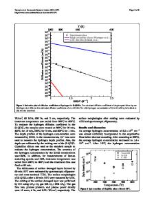
Abstract The use of gettering techniques, with precise location of the gettering regions, has become crucial for device manufacturing. Helium-induced cavities have been shown to getter metallic impurities very effectively, but suffer from the drawback of requiring relatively high He doses. In this work, He-implanted Cz wafers of varying resistivity were subjected to hydrogen plasma hydrogenation prior to the cavity-formation anneal. We focus our studies on the cavity layer interactions with metal impurities. XTEM images reveal that hydrogenation increases the cavity radius. Our SIMS results show that the doping level has no influence on the metal gettering efficiency while the addition of plasma hydrogenation tends to decrease it. However, the efficiency can be controlled with the cavity radius which is interesting for future applications of the technique.
Introduction The light elements, hydrogen and helium, are commonly used in semiconductor technology. Hydrogen exhibits extraordinary chemical activity in silicon, reacting with point and extended defects, surfaces and impurities. Effects such as passivation of pre-existing defects, and formation of new shallow and deep centers due to the presence of hydrogen in silicon are among the many well-known phenomena [1,2]. Helium is also used in silicon for gettering and minority carrier lifetime control applications [3-6]. High dose He implantation followed by thermal anneal results in the formation of a buried layer of nm-size cavities, whose large internal surfaces act as excellent gettering sites for fastdiffusing metallic impurities[3,4]. These defects strongly interact not only with metal impurities, but also with the dopant, affecting significantly their final profile and probably the electrical behavior of the device [4,5]. A clear understanding of the cavity formation and evolution is then required in order to safely introduce them in a device component. While many studies have shown that the presence of interstitial-type defects can lead to the shrinkage of He-cavities due to the interstitial capture by the cavities [6-8], there have so far been few reports dealing on the interaction of He-cavities with vacancies [9]. Plasma hydrogenation is widely encountered in semiconductor technology during various etching, deposition and passivation steps. It is well known that both defects and hydrogen atoms are injected into the subsurface layer under these conditions [10,11]. In previous work, we have demonstrated that additional H plasma treatment greatly impacts the morphology and size distribution o
Data Loading...