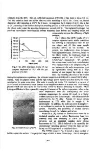
Optical Activation of Erbium Doped Porous Silicon by Hydrogen Plasma Treatment
- PDF / 374,717 Bytes
- 6 Pages / 414.72 x 648 pts Page_size
- 116 Downloads / 342 Views
ABSTRACT Er 3 +-doped porous silicon (Er:PS) shows strong room temperature emissions at - 1.54jpm. However, its spectrum is usually much broader than that of Er-doped crystalline silicon (fullwidth at half maximum - FWHM - is - 10 nm). It is probably because Er ions are located in amorphous phases. We report in this paper that strong and very sharp Er 3+ 1.54yrm emissions are obtained, when Er:PS samples are treated in a hydrogen plasma. Porous silicon layers are formed by anodic etching and then doped with Er3 + ions in an ErCl 3 /ethanol solution by an electrochemical method, and then treated in a hydrogen plasma at - 1000'C from 0.5 min to 90 min for the optical activation. Several sharp peaks are observed at 20K, of which the strongest peak is located at 1.538 /im with an FWHM less than 1 nm. This value is comparable to that obtained from Er3 +-doped crystalline silicon formed by means of molecular beam epitaxy (MBE) or ion implantation. Comparisons are made among hydrogen plasma, argon plasma, H2 flow and vacuum for the post-dope annealing atmosphere. Fourier-transform infrared (FT-IR) absorption and secondary ions mass spectrometry (SIMS) measurements are also carried out. We conclude that preferential etching of amorphous surface layers, and termination of dangling bonds of silicon nanocrystallites
with hydrogen atoms and formation of Er-H complexes may be responsible for the strong and sharp ErS+-related luminescence.
INTRODUCTION Sharp luminescence peaks from rare-earth ions doped in semiconductors have been attracting increasing attention [1][2], especially the 1.54pm luminescence peak from erbium ions due to a possibility of realizing a light-emitting diode or a laser diode as a light source of the optical fiber communication systems. However, its low emission efficiency and large thermal quenching make the operation at room temperature difficult. The authors' group has shown for the first time that Er3 + ions are very easily incorporated into porous silicon layers (PSLs) by an electrochemical method and that a strong roomtemperature luminescence of Er-related 1.54 pum peaks is obtained [6]. Effective widening of the bandgap of Si due to the quantum size effect [3] as well as the formation of Er-O complexes [4][5] is speculated to be the cause of the small thermal quenching. Er doping of porous silicon (PS) has also been carried out by Er spin coating [7], Er-ion implantation [8][9] or simply immersing of PS into an ErCla/C 2 H5OH saturated solution [10], followed by annealing in 02, N2 or in other ambients at high temperatures. How287 Mat. Res. Soc. Symp. Proc. Vol. 486 ©1998 Materials Research Society
ever, the Er-related 1.54 pm luminescence spectrum from Er-doped non-crystalline silicon is generally very broad. It is speculated that amorphous matrices of Er-doped regions or oxidation of Er(formation of Er 203) may cause Er ions to feel various crystal fields, leading to a broad luminescence spectrum. We demonstrate that annealing of Er-doped porous Si in a hydrogen atmosphere is effective for the
Data Loading...