Improved Aluminum Nitride Thin Films Grown by MOCVD from Tritertiarybutylaluminum and Ammonia
- PDF / 983,474 Bytes
- 6 Pages / 414.72 x 648 pts Page_size
- 80 Downloads / 321 Views
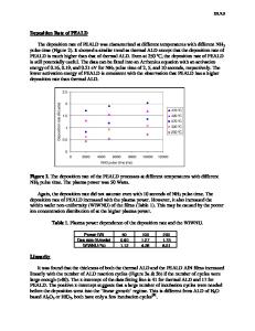
structures in order to investigate the influence of an AIN sublayer with varying thickness on the optical and structural properties of a GaN layer. EXPERIMENT AIN films with a thickness of 0.3 /im were grown by metalorganic chemical vapor deposition (MOCVD) from tritertiarybutylaluminum (TTBA) and ammonia (NH 3 ) on c-plane sapphire without a buffer-layer in a horizontal cold wall reactor. The growth temperature was 1050 TC and the deposition pressure was 100 mbar. Using hydrogen as transport gas the TTBA flux was maintained at 2.7 /Amol/min. To investigate the structural properties of the AIN thin films, high resolution X-ray diffraction (HRXRD) and atomic force microscopy (AFM) was applied. A modified triple axis diffractometer, which enables the recording of weak reflections, equipped with a graded multilayer mirror (Gobel mirror) [8] and two four-bounce Ge(220) channel cut crystals as incident beam optics and a second G6bel mirror for the diffracted beam optics was used. The Gobel mirror installed in front of the detector limits the angular acceptance of the detector to -60 arcsec. Both the symmetric 002 reflection and the asymmetric 105 reflection were measured with CuKc1 radiation in o-20-scan mode as well as in o-scan mode. For further structural investigations the samples were imaged by atomic force microscopy. The position of the optical bandgap as well as the sub-bandgap absorption of the thin AIN films was analyzed by photothermal deflection spectroscopy (PDS) in the energy range from 0.9 to 6.5 eV. With this method it is possible to determine absorption coefficients as low as oc = 0.1 cm- 1 for 1 m thick films. The experimental details are described elsewhere [9,10]. In order to investigate the influence of an increasing AIN layer thickness on the optical and structural properties of GaN, A1N/GaN-heterostructures were grown. AIN layers with variable thickness of 0.02, 0.06, 0.18, 0.25 and 0.36 /m were deposited on c-plane sapphire without a buffer layer as mentioned above. Subsequently GaN layers with a constant thickness of 0.75 psm were grown using triethylgallium (TEG) and NH 3 at a temperature of 950'C and a pressure of 100 mbar with growth rates of about 1.5 pm/h. Photoluminescence-(PL)-spectra of GaN were measured with the 333.2 nm line of an Ar+laser operating at an excitation power of 0.25 mW. Recording several reflections of GaN, the lattice constant co of the GaN films was determined by XRD with a Philips PW3040 diffractometer using the CuKox1 line. Raman spectra of the GaN layers were recorded with a micro-Raman system operating in back scattering geometry, where the 514.5 nm line of an Ar+ laser was focused through an orifice and a microscope on the GaN films. RESULTS Fig. 1 shows a typical AFM-image of a 0.3 l•m thick AIN film grown on c-plane sapphire at 1050 'C without a buffer layer. The surface roughness is of the order of 12 nm (rmsroughness). Clearly visible are individual crystallites with an averaged size of 0.1 14m. The orientation of the crystallites follows the epitaxial relatio
Data Loading...